- 您現(xiàn)在的位置:買賣IC網(wǎng) > PDF目錄372926 > XPC850ZT80BU Microprocessor PDF資料下載
參數(shù)資料
| 型號(hào): | XPC850ZT80BU |
| 英文描述: | Microprocessor |
| 中文描述: | 微處理器 |
| 文件頁(yè)數(shù): | 9/76頁(yè) |
| 文件大小: | 825K |
| 代理商: | XPC850ZT80BU |
第1頁(yè)第2頁(yè)第3頁(yè)第4頁(yè)第5頁(yè)第6頁(yè)第7頁(yè)第8頁(yè)當(dāng)前第9頁(yè)第10頁(yè)第11頁(yè)第12頁(yè)第13頁(yè)第14頁(yè)第15頁(yè)第16頁(yè)第17頁(yè)第18頁(yè)第19頁(yè)第20頁(yè)第21頁(yè)第22頁(yè)第23頁(yè)第24頁(yè)第25頁(yè)第26頁(yè)第27頁(yè)第28頁(yè)第29頁(yè)第30頁(yè)第31頁(yè)第32頁(yè)第33頁(yè)第34頁(yè)第35頁(yè)第36頁(yè)第37頁(yè)第38頁(yè)第39頁(yè)第40頁(yè)第41頁(yè)第42頁(yè)第43頁(yè)第44頁(yè)第45頁(yè)第46頁(yè)第47頁(yè)第48頁(yè)第49頁(yè)第50頁(yè)第51頁(yè)第52頁(yè)第53頁(yè)第54頁(yè)第55頁(yè)第56頁(yè)第57頁(yè)第58頁(yè)第59頁(yè)第60頁(yè)第61頁(yè)第62頁(yè)第63頁(yè)第64頁(yè)第65頁(yè)第66頁(yè)第67頁(yè)第68頁(yè)第69頁(yè)第70頁(yè)第71頁(yè)第72頁(yè)第73頁(yè)第74頁(yè)第75頁(yè)第76頁(yè)
MOTOROLA
MPC850 (Rev. A/B/C) Hardware Specifications
9
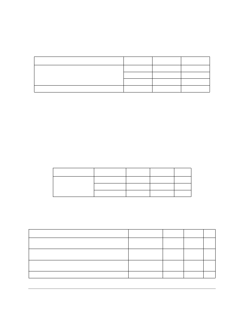
Part IV Thermal Characteristics
Table 4-3 shows the thermal characteristics for the MPC850.
Table 4-4 provides power dissipation information.
Table 4-5 provides the DC electrical characteristics for the MPC850.
Table 4-5. DC Electrical Specifications
Table 4-3. Thermal Characteristics
Characteristic
Symbol
Value
Unit
Thermal resistance for BGA
1
1
For more information on the design of thermal vias on multilayer boards and BGA layout considerations in
general, refer to AN-1231/D,
Plastic Ball Grid Array Application Note
office.
Assumes natural convection and a single layer board (no thermal vias).
Assumes natural convection, a multilayer board with thermal vias
temperature rise of 20
°
C above ambient.
Assumes natural convection, a multilayer board with thermal vias
temperature rise of 13
°
C above ambient.
T
J
= T
A
+ (P
D
P
D
= (V
DD
where:
P
I/O
is the power dissipation on pins
available from your local Motorola sales
θ
JA
40
2
2
3
°
C/W
θ
JA
31
3
4
, 1 watt MPC850 dissipation, and a board
°
C/W
θ
JA
24
4
4
4
, 1 watt MPC850 dissipation, and a board
θ
JA
DD
)
) + P
I
I/O
°
C/W
Thermal Resistance for BGA (junction-to-case)
θ
JC
8
°
C/W
Table 4-4. Power Dissipation (P
D
)
Characteristic
Frequency (MHz)
Typical
1
1
Typical power dissipation is measured at 3.3V
Maximum power dissipation is measured at 3.65 V
Maximum
2
2
Unit
Power Dissipation
All Revisions
(1:1) Mode
33
TBD
515
mW
40
TBD
590
mW
50
TBD
725
mW
Characteristic
Symbol
Min
Max
Unit
Operating voltage at 40 MHz or less
VDDH, VDDL,
KAPWR, VDDSYN
3.0
3.6
V
Operating voltage at 40 MHz or higher
VDDH, VDDL,
KAPWR, VDDSYN
3.135
3.465
V
Input high voltage (address bus, data bus, EXTAL, EXTCLK,
and all bus control/status signals)
VIH
2.0
3.6
V
Input high voltage (all general purpose I/O and peripheral pins)
VIH
2.0
5.5
V
相關(guān)PDF資料 |
PDF描述 |
|---|---|
| XPC855TZP80 | Controller Miscellaneous - Datasheet Reference |
| XPC860CZP50C1 | COMMUNICATIONS CONTROLLER |
| XPC860DCCZP33C1 | COMMUNICATIONS CONTROLLER |
| XPC860DCCZP50C1 | COMMUNICATIONS CONTROLLER |
| XPC860DCZP25 | Communications Controller |
相關(guān)代理商/技術(shù)參數(shù) |
參數(shù)描述 |
|---|---|
| XPC855TCZP50D4 | 制造商:MOTOROLA 制造商全稱:Motorola, Inc 功能描述:Family Hardware Specifications |
| XPC855TCZP66D4 | 制造商:MOTOROLA 制造商全稱:Motorola, Inc 功能描述:Family Hardware Specifications |
| XPC855TZP50 | 制造商:未知廠家 制造商全稱:未知廠家 功能描述:Controller Miscellaneous - Datasheet Reference |
| XPC855TZP50D4 | 制造商:Motorola Inc 功能描述: |
| XPC855TZP66D4 | 制造商:MOTOROLA 制造商全稱:Motorola, Inc 功能描述:Family Hardware Specifications |
發(fā)布緊急采購(gòu),3分鐘左右您將得到回復(fù)。