- 您現(xiàn)在的位置:買賣IC網(wǎng) > PDF目錄375007 > XCF32PVOG48 (Xilinx, Inc.) Platform Flash In-System Programmable Configuration PROMS PDF資料下載
參數(shù)資料
| 型號: | XCF32PVOG48 |
| 廠商: | Xilinx, Inc. |
| 英文描述: | Platform Flash In-System Programmable Configuration PROMS |
| 中文描述: | 平臺Flash在系統(tǒng)可編程配置方案管理系統(tǒng) |
| 文件頁數(shù): | 39/46頁 |
| 文件大小: | 525K |
| 代理商: | XCF32PVOG48 |
第1頁第2頁第3頁第4頁第5頁第6頁第7頁第8頁第9頁第10頁第11頁第12頁第13頁第14頁第15頁第16頁第17頁第18頁第19頁第20頁第21頁第22頁第23頁第24頁第25頁第26頁第27頁第28頁第29頁第30頁第31頁第32頁第33頁第34頁第35頁第36頁第37頁第38頁當前第39頁第40頁第41頁第42頁第43頁第44頁第45頁第46頁
Platform Flash In-System Programmable Configuration PROMS
DS123 (v2.9) May 09, 2006
www.xilinx.com
39
R
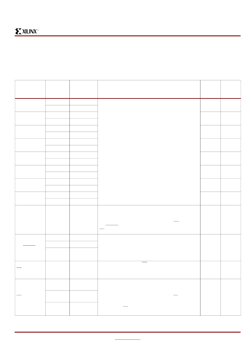
XCFxxP Pinouts and Pin Descriptions
VXCFxxP O48/VOG48 and FS48/FSG48 Pin Names and Descriptions
Table 14
provides a list of the pin names and descriptions for the XCFxxP 48-pin VO48/VOG48 and 48-pin FS48/FSG48
packages.
Table 14:
XCFxxP Pin Names and Descriptions (VO48/VOG48 and FS48/FSG48)
Pin Name
Boundary
Scan Order
Boundary
Scan
Function
Pin Description
48-pin
TSOP
(VO48/
VOG48)
48-pin
TFBGA
(FS48/
FSG48)
D0
28
Data Out
D0 is the DATA output pin to provide data for configuring an
FPGA in serial mode.
D0-D7 are the DATA output pins to provide parallel data for
configuring a Xilinx FPGA in SelectMap (parallel) mode.
The D0 output is set to a high-impedance state during ISPEN
(when not clamped).
The D1-D7 outputs are set to a high-impedance state during
ISPEN (when not clamped) and when serial mode is selected
for configuration. The D1-D7 pins can be left unconnected
when the PROM is used in serial mode.
28
H6
27
Output Enable
D1
26
Data Out
29
H5
25
Output Enable
D2
24
Data Out
32
E5
23
Output Enable
D3
22
Data Out
33
D5
21
Output Enable
D4
20
Data Out
43
C5
19
Output Enable
D5
18
Data Out
44
B5
17
Output Enable
D6
16
Data Out
47
A5
15
Output Enable
D7
14
Data Out
48
A6
13
Output Enable
CLK
01
Data In
Configuration Clock Input. An internal programmable control
bit selects between the internal oscillator and the CLK input
pin as the clock source to control the configuration sequence.
Each rising edge on the CLK input increments the internal
address counter if the CLK input is selected, CE is Low,
OE/RESET is High, BUSY is Low (parallel mode only), and
CF is High.
12
B3
OE/RESET
04
Data In
Output Enable/Reset (Open-Drain I/O).
When Low, this input holds the address counter reset and the
DATA and CLKOUT outputs are placed in a high-impedance
state. This is a bidirectional open-drain pin that is held Low
while the PROM completes the internal power-on reset
sequence. Polarity is not programmable.
11
A3
03
Data Out
02
Output Enable
CE
00
Data In
Chip Enable Input. When CE is High, the device is put into
low-power standby mode, the address counter is reset, and
the DATA and CLKOUT outputs are placed in a
high-impedance state.
13
B4
CF
11
Data In
Configuration Pulse (Open-Drain I/O). As an output, this pin
allows the JTAG CONFIG instruction to initiate FPGA
configuration without powering down the FPGA. This is an
open-drain signal that is pulsed Low by the JTAG CONFIG
command. As an input, on the rising edge of CF, the current
design revision selection is sampled and the internal address
counter is reset to the start address for the selected revision.
If unused, the CF pin must be pulled High using an external
4.7 K
Ω
pull-up to V
CCO
.
6
D1
10
Data Out
09
Output Enable
相關PDF資料 |
PDF描述 |
|---|---|
| XCF32PVOG48C | Platform Flash In-System Programmable Configuration PROMS |
| XCR22LV10-10SO24C | 20 characters x 2 Lines, 5x7 Dot Matric Character and Cursor |
| XCR22LV10-10SO24I | 20 characters x 2 Lines, 5x7 Dot Matric Character and Cursor |
| XCR22LV10 | TotalCMOS, Universal PLD Device |
| XCR22LV10-10PC28C | TotalCMOS, Universal PLD Device |
相關代理商/技術參數(shù) |
參數(shù)描述 |
|---|---|
| XCF32PVOG48C | 功能描述:IC PROM SRL 1.8V 32M GATE 48TSOP RoHS:是 類別:集成電路 (IC) >> 存儲器 - 用于 FPGA 的配置 Proms 系列:- 產(chǎn)品變化通告:Product Discontinuation 28/Jul/2010 標準包裝:98 系列:- 可編程類型:OTP 存儲容量:300kb 電源電壓:3 V ~ 3.6 V 工作溫度:-40°C ~ 85°C 封裝/外殼:8-SOIC(0.154",3.90mm 寬) 供應商設備封裝:8-TSOP 包裝:管件 |
| XCF32PVOG48C0936 | 制造商:Xilinx 功能描述:XLXXCF32PVOG48C0936 PROM |
| XCF32PVOG48C4118 | 制造商:Xilinx 功能描述: |
| XCF3-81 | 制造商:SAIA - BURGESS ELECTRONICS INC. 功能描述:Catalogue / XCF3-81 |
| XCF3-81-J1 | 制造商:SAIA - BURGESS ELECTRONICS INC. 功能描述:Catalogue / XCF3-81-J1 |
發(fā)布緊急采購,3分鐘左右您將得到回復。