- 您現(xiàn)在的位置:買(mǎi)賣(mài)IC網(wǎng) > PDF目錄375007 > XCF08PVO48C (XILINX INC) Platform Flash In-System Programmable Configuration PROMS PDF資料下載
參數(shù)資料
| 型號(hào): | XCF08PVO48C |
| 廠商: | XILINX INC |
| 元件分類(lèi): | DRAM |
| 英文描述: | Platform Flash In-System Programmable Configuration PROMS |
| 中文描述: | 8M X 1 CONFIGURATION MEMORY, PDSO48 |
| 封裝: | PLASTIC, TSOP-48 |
| 文件頁(yè)數(shù): | 22/46頁(yè) |
| 文件大小: | 525K |
| 代理商: | XCF08PVO48C |
第1頁(yè)第2頁(yè)第3頁(yè)第4頁(yè)第5頁(yè)第6頁(yè)第7頁(yè)第8頁(yè)第9頁(yè)第10頁(yè)第11頁(yè)第12頁(yè)第13頁(yè)第14頁(yè)第15頁(yè)第16頁(yè)第17頁(yè)第18頁(yè)第19頁(yè)第20頁(yè)第21頁(yè)當(dāng)前第22頁(yè)第23頁(yè)第24頁(yè)第25頁(yè)第26頁(yè)第27頁(yè)第28頁(yè)第29頁(yè)第30頁(yè)第31頁(yè)第32頁(yè)第33頁(yè)第34頁(yè)第35頁(yè)第36頁(yè)第37頁(yè)第38頁(yè)第39頁(yè)第40頁(yè)第41頁(yè)第42頁(yè)第43頁(yè)第44頁(yè)第45頁(yè)第46頁(yè)
Platform Flash In-System Programmable Configuration PROMS
DS123 (v2.9) May 09, 2006
www.xilinx.com
22
R
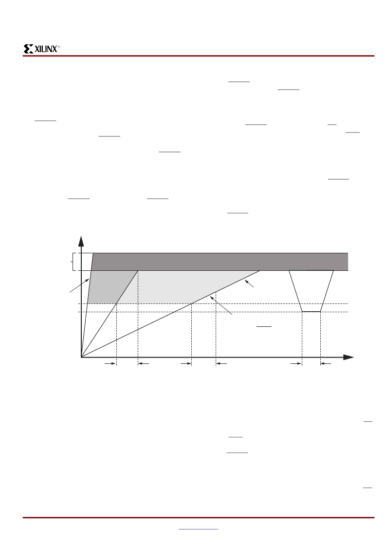
Reset and Power-On Reset Activation
At power up, the device requires the V
CCINT
power supply to
monotonically rise to the nominal operating voltage within
the specified V
CCINT
rise time. If the power supply cannot
meet this requirement, then the device might not perform
power-on reset properly. During the power-up sequence,
OE/RESET is held Low by the PROM. Once the required
supplies have reached their respective POR (Power On
Reset) thresholds, the OE/RESET release is delayed (T
OER
minimum) to allow more margin for the power supplies to
stabilize before initiating configuration. The OE/RESET pin
is connected to an external 4.7k
Ω
pull-up resistor and also
to the target FPGA's INIT pin. For systems utilizing
slow-rising power supplies, an additional power monitoring
circuit can be used to delay the target configuration until the
system power reaches minimum operating voltages by
holding the OE/RESET pin Low. When OE/RESET is
released, the FPGA’s INIT pin is pulled High allowing the
FPGA's configuration sequence to begin. If the power drops
below the power-down threshold (V
CCPD
), the PROM resets
and OE/RESET is again held Low until the after the POR
threshold is reached. OE/RESET polarity is not
programmable. These power-up requirements are shown
graphically in
Figure 14, page 22
.
For a fully powered Platform Flash PROM, a reset occurs
whenever OE/RESET is asserted (Low) or CE is
deasserted (High). The address counter is reset, CEO is
driven High, and the remaining outputs are placed in a
high-impedance state.
Notes:
1.
The XCFxxS PROM only requires V
CCINT
to rise above
its POR threshold before releasing OE/RESET.
The XCFxxP PROM requires both V
CCINT
to rise above
its POR threshold and for V
CCO
to reach the
recommended operating voltage level before releasing
OE/RESET.
2.
I/O Input Voltage Tolerance and Power Sequencing
The I/Os on each re-programmable Platform Flash PROM
are fully 3.3V-tolerant. This allows 3V CMOS signals to
connect directly to the inputs without damage. The core
power supply (V
CCINT
), JTAG pin power supply (V
CCJ
),
output power supply (V
CCO
), and external 3V CMOS I/O
signals can be applied in any order.
Additionally, for the XCFxxS PROM only, when V
CCO
is
supplied at 2.5V or 3.3V and V
CCINT
is supplied at 3.3V, the
I/Os are 5V-tolerant. This allows 5V CMOS signals to connect
directly to the inputs on a powered XCFxxS PROM without
damage. Failure to power the PROM correctly while supplying
a 5V input signal may result in damage to the XCFxxS device.
Standby Mode
The PROM enters a low-power standby mode whenever CE
is deasserted (High). In standby mode, the address counter
is reset, CEO is driven High, and the remaining outputs are
placed in a high-impedance state regardless of the state of
the OE/RESET input. For the device to remain in the
low-power standby mode, the JTAG pins TMS, TDI, and
TDO must not be pulled Low, and TCK must be stopped
(High or Low).
When using the FPGA DONE signal to drive the PROM CE
pin High to reduce standby power after configuration, an
external pull-up resistor should be used. Typically a 330
Ω
Figure 14:
Platform Flash PROM Power-Up Requirements
T
OER
V
CCINT
V
CCPOR
V
CCPD
200 μ
s
r
a
mp
50 m
s
r
a
mp
T
OER
T
R
S
T
TIME (m
s
)
A
s
low-r
a
mping V
CCINT
su
pply m
a
y
s
till
b
e
b
elow the minim
u
m oper
a
ting
volt
a
ge when OE/RE
S
ET i
s
rele
as
ed.
In thi
s
c
as
e, the config
u
r
a
tion
s
e
qu
ence m
us
t
b
e del
a
yed
u
ntil
b
oth
V
CCINT
a
nd V
CCO
h
a
ve re
a
ched their
recommended oper
a
ting condition
s
.
Recommended Operatin
g
Ran
g
e
Delay or Re
s
tart
Confi
g
uration
d
s
12
3
_21_10
3
10
3
相關(guān)PDF資料 |
PDF描述 |
|---|---|
| XCF08PVOG48 | Platform Flash In-System Programmable Configuration PROMS |
| XCF08PVOG48C | Platform Flash In-System Programmable Configuration PROMS |
| XCF16P | Platform Flash In-System Programmable Configuration PROMS |
| XCF16PF48 | Platform Flash In-System Programmable Configuration PROMS |
| XCF16PFG48 | Platform Flash In-System Programmable Configuration PROMS |
相關(guān)代理商/技術(shù)參數(shù) |
參數(shù)描述 |
|---|---|
| XCF08PVO48C | 制造商:Xilinx 功能描述: |
| XCF08PVO48C0973 | 制造商:Rochester Electronics LLC 功能描述: 制造商:Xilinx 功能描述: |
| XCF08PVO48CES | 制造商:Xilinx 功能描述: |
| XCF08PVO48CESB | 制造商:Xilinx 功能描述: |
| XCF08PVOG48 | 制造商:XILINX 制造商全稱(chēng):XILINX 功能描述:Platform Flash In-System Programmable Configuration PROMS |
發(fā)布緊急采購(gòu),3分鐘左右您將得到回復(fù)。