- 您現(xiàn)在的位置:買賣IC網(wǎng) > PDF目錄374980 > XC3030A-7PC68I (XILINX INC) Field Programmable Gate Arrays (XC3000A/L, XC3100A/L) PDF資料下載
參數(shù)資料
| 型號: | XC3030A-7PC68I |
| 廠商: | XILINX INC |
| 元件分類: | FPGA |
| 英文描述: | Field Programmable Gate Arrays (XC3000A/L, XC3100A/L) |
| 中文描述: | FPGA, 100 CLBS, 1500 GATES, 113 MHz, PQCC68 |
| 封裝: | PLASTIC, LCC-68 |
| 文件頁數(shù): | 57/76頁 |
| 文件大小: | 731K |
| 代理商: | XC3030A-7PC68I |
第1頁第2頁第3頁第4頁第5頁第6頁第7頁第8頁第9頁第10頁第11頁第12頁第13頁第14頁第15頁第16頁第17頁第18頁第19頁第20頁第21頁第22頁第23頁第24頁第25頁第26頁第27頁第28頁第29頁第30頁第31頁第32頁第33頁第34頁第35頁第36頁第37頁第38頁第39頁第40頁第41頁第42頁第43頁第44頁第45頁第46頁第47頁第48頁第49頁第50頁第51頁第52頁第53頁第54頁第55頁第56頁當(dāng)前第57頁第58頁第59頁第60頁第61頁第62頁第63頁第64頁第65頁第66頁第67頁第68頁第69頁第70頁第71頁第72頁第73頁第74頁第75頁第76頁
R
November 9, 1998 (Version 3.1)
7-59
XC3000 Series Field Programmable Gate Arrays
7
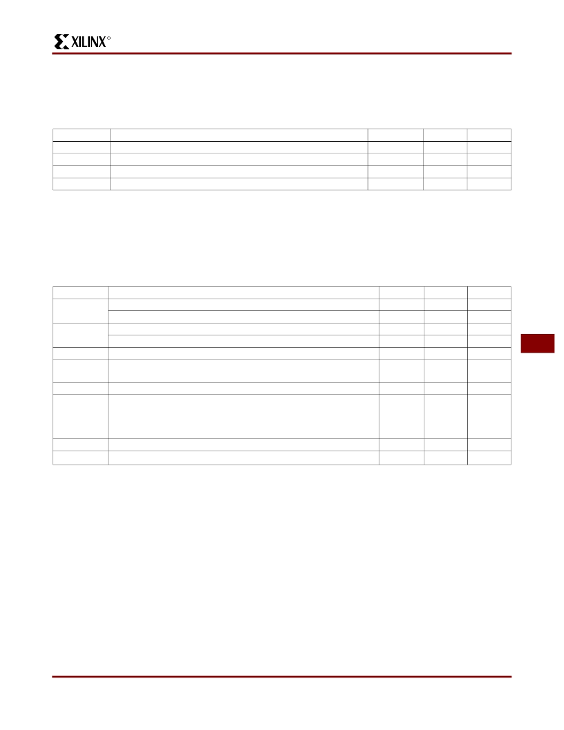
XC3100L Switching Characteristics
Xilinx maintains test specifications for each product as controlled documents. To insure the use of the most recently released
device performance parameters, please request a copy of the current test-specification revision.
XC3100L Operating Conditions
Notes:
1. At junction temperatures above those listed as Operating Conditions, all delay parameters increase by 0.3% per
°
C.
2. Although the present (1996) devices operate over the full supply voltage range from 3.0 V to 5.25 V, Xilinx reserves the right
to restrict operation to the 3.0 and 3.6 V range later, when smaller device geometries might preclude operation @ 5 V.
Operating conditions are guaranteed in the 3.0 – 3.6 V V
CC
range.
XC3100L DC Characteristics Over Operating Conditions
Notes:
1. With no output current loads, no active input or long line pull-up resistors, all package pins at V
CC
or GND, and the FPGA
configured with a tie option.
2. Total continuous output sink current may not exceed 100 mA per ground pin. Total continuous output source current may not
exceed 100 mA per V
CC
pin. The number of ground pins varies from the XC3142L to the XC3190L.
3. Not tested. Allows undriven pins to float High. For any other purpose, use an external pull-up.
Symbol
V
CC
V
IH
V
IL
T
IN
Description
Min
3.0
2.0
-0.3
Max
3.6
Units
V
V
V
ns
Supply voltage relative to GND Commercial 0
°
C to +85
°
C junction
High-level input voltage
Low-level input voltage
Input signal transition time
V
CC
+ 0.3
0.8
250
Symbol
Description
Min
2.4
Max
Units
V
V
V
V
V
mA
V
OH
High-level output voltage (@ I
OH
= -4.0 mA, V
CC
min)
High-level output voltage (@ I
OH
= -100.0
μ
A, V
CC
min)
Low-level output voltage (@ I
OH
= 4.0 mA, V
CC
min)
Low-level output voltage (@ I
OH
= +100.0
μ
A, V
CC
min)
Power-down supply voltage (PWRDWN must be Low)
Quiescent FPGA supply current
Chip thresholds programmed as CMOS levels
1
Input Leakage Current
Input capacitance
(sample tested)
All pins except XTL1 and XTL2
XTL1 and XTL2
Pad pull-up (when selected) @ V
IN
= 0 V
3
Horizontal long line pull-up (when selected) @ logic Low
V
CC
-0.2
V
OL
0.40
0.2
V
CCPD
I
CCO
2.30
1.5
I
IL
-10
+10
μ
A
C
IN
10
15
0.17
2.80
pF
pF
mA
mA
I
RIN
I
RLL
0.02
0.20
相關(guān)PDF資料 |
PDF描述 |
|---|---|
| XC3030A-7PC84I | Field Programmable Gate Arrays (XC3000A/L, XC3100A/L) |
| XC3030A-7VQ64C | Field Programmable Gate Arrays (XC3000A/L, XC3100A/L) |
| XC3030L-8PC84C | Field Programmable Gate Arrays (XC3000A/L, XC3100A/L) |
| XC3030L-8PC84I | Field Programmable Gate Arrays (XC3000A/L, XC3100A/L) |
| XC3043L | Field Programmable Gate Arrays(現(xiàn)場可編程門陣列) |
相關(guān)代理商/技術(shù)參數(shù) |
參數(shù)描述 |
|---|---|
| XC3030A-7PC68I0280 | 制造商:Xilinx 功能描述: |
| XC3030A-7PC84C | 功能描述:IC LOGIC CL ARRAY 3000GAT 84PLCC RoHS:否 類別:集成電路 (IC) >> 嵌入式 - FPGA(現(xiàn)場可編程門陣列) 系列:XC3000A/L 產(chǎn)品變化通告:XC4000(E,L) Discontinuation 01/April/2002 標(biāo)準(zhǔn)包裝:24 系列:XC4000E/X LAB/CLB數(shù):100 邏輯元件/單元數(shù):238 RAM 位總計(jì):3200 輸入/輸出數(shù):80 門數(shù):3000 電源電壓:4.5 V ~ 5.5 V 安裝類型:表面貼裝 工作溫度:-40°C ~ 100°C 封裝/外殼:120-BCBGA 供應(yīng)商設(shè)備封裝:120-CPGA(34.55x34.55) |
| XC3030A-7PC84C0100 | 制造商:Xilinx 功能描述: |
| XC3030A-7PC84I | 制造商:XILINX 制造商全稱:XILINX 功能描述:Field Programmable Gate Arrays (XC3000A/L, XC3100A/L) |
| XC3030A-7PQ100C | 功能描述:IC LOGIC CL ARRAY 3000GAT 100PQF RoHS:否 類別:集成電路 (IC) >> 嵌入式 - FPGA(現(xiàn)場可編程門陣列) 系列:XC3000A/L 產(chǎn)品變化通告:XC4000(E,L) Discontinuation 01/April/2002 標(biāo)準(zhǔn)包裝:24 系列:XC4000E/X LAB/CLB數(shù):100 邏輯元件/單元數(shù):238 RAM 位總計(jì):3200 輸入/輸出數(shù):80 門數(shù):3000 電源電壓:4.5 V ~ 5.5 V 安裝類型:表面貼裝 工作溫度:-40°C ~ 100°C 封裝/外殼:120-BCBGA 供應(yīng)商設(shè)備封裝:120-CPGA(34.55x34.55) |
發(fā)布緊急采購,3分鐘左右您將得到回復(fù)。