- 您現(xiàn)在的位置:買賣IC網(wǎng) > PDF目錄359439 > VT82885 (Electronic Theatre Controls, Inc.) Real Time Clock PDF資料下載
參數(shù)資料
| 型號: | VT82885 |
| 廠商: | Electronic Theatre Controls, Inc. |
| 英文描述: | Real Time Clock |
| 中文描述: | 實(shí)時(shí)時(shí)鐘 |
| 文件頁數(shù): | 5/16頁 |
| 文件大小: | 72K |
| 代理商: | VT82885 |
5
VT82885
Real Time Clock
VIA Technologies, Inc.
E. Periodic Interrupt Flag (PF) bit is cleared
to zero.
F.
The device is not accessible until
RESET# is returned high.
G. Alarm Interrupt Flag (AF) bit is cleared to
zero.
H. IRQ# pin is in the high impedence state.
I.
Square Wave Output Enable (SQWE)
bit is cleared to zero.
J.
Update Ended Interrupt Enable (UIE) is
cleared to zero.
In a typical application RESET# can be
connected to V
CC
. This connection will allow
the VT82885 to go in and out of power fail
without affecting any of the control registers.
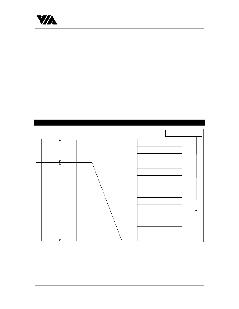
ADDRESS MAP
The address map of the VT82885 is shown
in Figure 2. The address map consists of
114 bytes of user RAM, 10 bytes of RAM
that contain the RTC time, calendar and
alarm data, and four bytes which are used
for control and status. All 128 bytes can be
directly written or read except the following:
1.
Registers C and D are read-only.
2.
Bit 7 of Register A is read-only.
3.
The high order bit of the seconds byte is
read-only.
The contents of four registers (A, B, C and
D) are described in the “Register” section.
FIGURE 2: ADDRESS MAP VT82885
TIME, CALENDAR AND ALARM
LOCATIONS
The time and calendar information is
obtained by reading the appropriate memory
bytes. The time, calendar and alarm are set
or initialized by writing the appropriate RAM
bytes. The contents of the ten time, calen-
dar and alarm bytes can be either Binary or
Binary-Coded Decimal (BCD) format. Be-
fore writing the internal time, calendar and
alarm registers, the SET bit in Register B
0
SECONDS
00
1
SECONDS ALARM
01
2
MINUTES
02
3
MINUTES ALARM
03
4
HOURS
04
5
HOURS ALARM
05
6
DAY OF THE WEEK
06
7
DAY OF THE MONTH
07
8
MONTH
08
9
YEAR
09
10
REGISTER A
0A
11
REGISTER B
0B
12
REGISTER C
0C
13
REGISTER D
0D
127
0
00
OD
0E
13
14
7F
14 Bytes
Clock and Control
Status Registers
114 Bytes
Storage
Registers
Binary or BCD Input
相關(guān)PDF資料 |
PDF描述 |
|---|---|
| VT82C42 | VT82C42 Keyboard Controller |
| VT82C586A | PIC Integrated Peripheral Controller |
| VT82C586B | PCI INTEGRATED PERIPHERAL CONTROLLER |
| VT82C686A | PCI SUPER-I/O INTEGRATED PERIPHERAL CONTROLLER |
| vt82c693 | APOLLO PRO-PLUS |
相關(guān)代理商/技術(shù)參數(shù) |
參數(shù)描述 |
|---|---|
| VT82885(24DIP) | 制造商:未知廠家 制造商全稱:未知廠家 功能描述:Real-Time Clock |
| VT82885(28PLCC) | 制造商:未知廠家 制造商全稱:未知廠家 功能描述:Real-Time Clock |
| VT82887 | 制造商:未知廠家 制造商全稱:未知廠家 功能描述:Real Time Clock |
| VT82A192 | 制造商:未知廠家 制造商全稱:未知廠家 功能描述: |
| VT82C42 | 制造商:未知廠家 制造商全稱:未知廠家 功能描述:VT82C42 Keyboard Controller |
發(fā)布緊急采購,3分鐘左右您將得到回復(fù)。