- 您現(xiàn)在的位置:買賣IC網(wǎng) > PDF目錄297781 > VSKU105/12S90P (VISHAY INTERTECHNOLOGY INC) 165 A, 1200 V, SCR, TO-240AA PDF資料下載
參數(shù)資料
| 型號: | VSKU105/12S90P |
| 廠商: | VISHAY INTERTECHNOLOGY INC |
| 元件分類: | 晶閘管 |
| 英文描述: | 165 A, 1200 V, SCR, TO-240AA |
| 封裝: | ROHS COMPLIANT, ADD-A-PAK-7 |
| 文件頁數(shù): | 3/8頁 |
| 文件大?。?/td> | 163K |
| 代理商: | VSKU105/12S90P |
Document Number: 94423
For technical questions, contact: ind-modules@vishay.com
www.vishay.com
Revision: 24-Apr-08
3
VSKU/V105..PbF Series
Thyristor/Thyristor, 105 A
(ADD-A-PAKTM Generation 5 Power Modules)
Vishay High Power Products
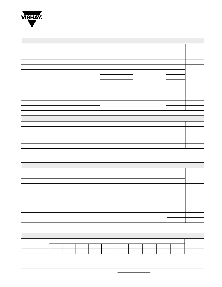
Note
(1) Available with dV/dt = 1000 V/s, to complete code add S90 i.e. VSKU105/16AS90
Note
Table shows the increment of thermal resistance RthJC when devices operate at different conduction angles than DC
TRIGGERING
PARAMETER
SYMBOL
TEST CONDITIONS
VALUES
UNITS
Maximum peak gate power
PGM
12
W
Maximum average gate power
PG(AV)
3
Maximum peak gate current
IGM
3A
Maximum peak negative gate voltage
- VGM
10
V
Maximum gate voltage required to trigger
VGT
TJ = - 40 °C
Anode supply = 6 V
resistive load
4.0
TJ = 25 °C
2.5
TJ = 125 °C
1.7
Maximum gate current required to trigger
IGT
TJ = - 40 °C
Anode supply = 6 V
resistive load
270
mA
TJ = 25 °C
150
TJ = 125 °C
80
Maximum gate voltage that will not trigger
VGD
TJ = 125 °C, rated VDRM applied
0.25
V
Maximum gate current that will not trigger
IGD
6mA
BLOCKING
PARAMETER
SYMBOL
TEST CONDITIONS
VALUES
UNITS
Maximum peak reverse and off-state leakage
current at VRRM, VDRM
IRRM,
IDRM
TJ = 130 °C, gate open circuit
20
mA
RMS insulation voltage
VINS
50 Hz, circuit to base, all terminals shorted
2500 (1 min)
3500 (1 s)
V
Maximum critical rate of rise of off-state voltage
dV/dt (1)
TJ = 130 °C, linear to 0.67 VDRM, gate open circuit
500
V/s
THERMAL AND MECHANICAL SPECIFICATIONS
PARAMETER
SYMBOL
TEST CONDITIONS
VALUES
UNITS
Junction operating temperature range
TJ
- 40 to 130
°C
Storage temperature range
TStg
- 40 to 125
Maximum internal thermal resistance,
junction to case per module
RthJC
DC operation
0.135
K/W
Typical thermal resistance, case to heatsink
RthCS
Mounting surface flat, smooth and greased
0.1
Mounting torque ± 10 %
to heatsink
A mounting compound is recommended and
the torque should be rechecked after a period of
3 hours to allow for the spread of the compound.
5
Nm
busbar
3
Approximate weight
110
g
4oz.
Case style
JEDEC
TO-240AA
ΔR CONDUCTION PER JUNCTION
DEVICES
SINE HALF WAVE CONDUCTION
RECTANGULAR WAVE CONDUCTION
UNITS
180°
120°
90°
60°
30°
180°
120°
90°
60°
30°
VSKU/V105
0.04
0.05
0.06
0.08
0.12
0.03
0.05
0.06
0.08
0.12
°C/W
相關PDF資料 |
PDF描述 |
|---|---|
| VSKV71/08P | 115 A, 800 V, SCR, TO-240AA |
| VSKV71/08S90P | 115 A, 800 V, SCR, TO-240AA |
| VSKV71/08 | 115 A, 800 V, SCR, TO-240AA |
| VSLD61TJ3EN-65.536MHZ | VCXO, CLOCK, 65.536 MHz, HCMOS OUTPUT |
| VSM52251 | VCXO, CLOCK, 55.296 MHz, CMOS/TTL OUTPUT |
相關代理商/技術參數(shù) |
參數(shù)描述 |
|---|---|
| VSKU105-16 | 制造商:VISHAY 制造商全稱:Vishay Siliconix 功能描述:ADD-A-PAK Generation VII Power Modules Thyristor/Thyristor, 105 A |
| VSKU10516P | 制造商:VISHAY 制造商全稱:Vishay Siliconix 功能描述:Thyristor/Thyristor, 105 A (ADD-A-PAKTM Generation 5 Power Modules) |
| VSKU10516S90P | 制造商:VISHAY 制造商全稱:Vishay Siliconix 功能描述:Thyristor/Thyristor, 105 A (ADD-A-PAKTM Generation 5 Power Modules) |
| VSKU10616P | 制造商:VISHAY 制造商全稱:Vishay Siliconix 功能描述:Thyristor/Thyristor, 105 A (ADD-A-PAKTM Generation 5 Power Modules) |
| VSKU10616S90P | 制造商:VISHAY 制造商全稱:Vishay Siliconix 功能描述:Thyristor/Thyristor, 105 A (ADD-A-PAKTM Generation 5 Power Modules) |
發(fā)布緊急采購,3分鐘左右您將得到回復。