- 您現(xiàn)在的位置:買(mǎi)賣IC網(wǎng) > PDF目錄359317 > V29C51002B (Mosel Vitelic, Corp.) High Speed 2 MEGA Bit 5 Volt CMOS Flash Memory(高速2M位5V CMOS閃速存儲(chǔ)器) PDF資料下載
參數(shù)資料
| 型號(hào): | V29C51002B |
| 廠商: | Mosel Vitelic, Corp. |
| 英文描述: | High Speed 2 MEGA Bit 5 Volt CMOS Flash Memory(高速2M位5V CMOS閃速存儲(chǔ)器) |
| 中文描述: | 高速2兆的5伏的CMOS快閃記憶體(200萬(wàn)位高速5V的CMOS閃速存儲(chǔ)器) |
| 文件頁(yè)數(shù): | 10/16頁(yè) |
| 文件大小: | 82K |
| 代理商: | V29C51002B |
第1頁(yè)第2頁(yè)第3頁(yè)第4頁(yè)第5頁(yè)第6頁(yè)第7頁(yè)第8頁(yè)第9頁(yè)當(dāng)前第10頁(yè)第11頁(yè)第12頁(yè)第13頁(yè)第14頁(yè)第15頁(yè)第16頁(yè)
10
V29C51002T/V29C51002B Rev. 1.7 February
MOSEL V ITELIC
V29C51002T/V29C51002B
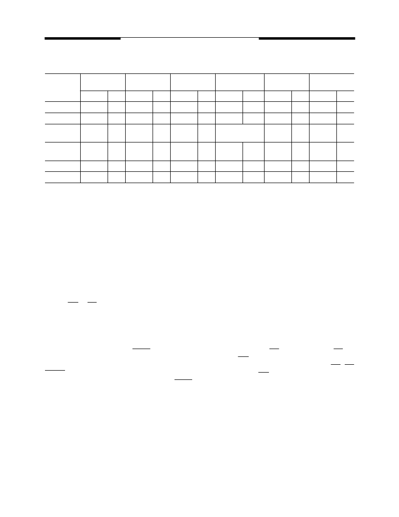
Table 2. Command Codes
NOTES:
1.
2.
3.
4.
5.
RA: Read Address
RD: Read Data
PA: The address of the memory location to be programmed.
PD: The data at the byte address to be programmed.
SA(5): Sector Address
Command
Sequence
First Bus
Program Cycle
Second Bus
Program Cycle
Third Bus
Program Cycle
Fourth Bus
Program Cycle
Fifth Bus
Program Cycle
Six Bus
Program Cycle
Address
Data
Address
Data
Address
Data
Address
Data
Address
Data
Address
Data
Read
XXXXH
F0H
Read
5555H
AAH
2AAAH
55H
5555H
F0H
RA(1)
RD(2)
Autoselect
Mode
5555H
AAH
2AAAH
55H
5555H
90H
See table 3 for detail.
Byte
Program
5555H
AAH
2AAAH
55H
5555H
A0H
PA
PD(4)
Chip Erase
5555H
AAH
2AAAH
55H
5555H
80H
5555H
AAH
2AAAH
55H
5555H
10H
Sector Erase
5555H
AAH
2AAAH
55H
5555H
80H
5555H
AAH
2AAAH
55H
SA(5)
30H
Chip Erase Cycle
The V29C51002T/V29C51002B features a chip-
erase operation. The chip erase operation is
initiated by using a specific six-bus-cycle
sequence: two unlock program cycles, a setup
command, two additional unlock program cycles,
and the chip erase command (see Table 2).
The automatic erase begins on the rising edge of
the last WE or CE pulse in the command sequence
and terminates when the data on DQ7 is “1”.
Program Cycle Status Detection
There are two methods for determining the state
of the V29C51002T/V29C51002B during a
program (erase/write) cycle: DATA Polling (I/O
7
)
and Toggle Bit (I/O
6
).
DATA Polling (I/O
7
)
The V29C51002T/V29C51002B features DATA
polling to indicate the end of a program cycle.
When the device is in the program cycle, any
attempt to read the device will received the
complement of the loaded data on I/O
7
. Once the
program cycle is completed, I/O
7
will show true
data, and the device is then ready for the next
cycle.
Toggle Bit (I/O
6
)
The V29C51002T/V29C51002B also features
another method for determining the end of a
program cycle. When the device is in the program
cycle, any attempt to read the device will result in
l/O
6
toggling between 1 and 0. Once the program is
completed, the toggling will stop. The device is then
ready for the next operation. Examining the toggle
bit may begin at any time during a program cycle.
Boot Block Protection Enabling/Disabling
The V29C51002T/V29C51002B features
hardware Boot Block Protection. The boot block
sector protection is enabled when high voltage
(12.5V) is applied to OE and A9 pins with CE pin
LOW and WE pin LOW. The sector protection is
disabled when high voltage is applied to OE, CE
and A9 pins with WE pin LOW. Other pins can be
HIGH or LOW. This is shown in table 1.
Autoselect Mode
The V29C51002T/V29C51002B features an
Autoselect mode to identify boot block locking
status, device ID and manufacturer ID.
Entering Autoselect mode is accomplished by
applying a high voltage (VH) to the A9 Pin, or
through a sequence of commands (as shown in
table 2). Device will exit this mode once high
voltage on A9 is removed or another command is
loaded into the device.
相關(guān)PDF資料 |
PDF描述 |
|---|---|
| V29C51004B-70J | x8 Flash EEPROM |
| V29C51004B-70T | x8 Flash EEPROM |
| V29C51004B-90J | x8 Flash EEPROM |
| V29C51004T-90T | x8 Flash EEPROM |
| V29C51004T-90J | x8 Flash EEPROM |
相關(guān)代理商/技術(shù)參數(shù) |
參數(shù)描述 |
|---|---|
| V29C51002B-55J | 制造商:MOSEL 制造商全稱:MOSEL 功能描述:2 MEGABIT 262,144 x 8 BIT 5 VOLT CMOS FLASH MEMORY |
| V29C51002B-55P | 制造商:MOSEL 制造商全稱:MOSEL 功能描述:2 MEGABIT 262,144 x 8 BIT 5 VOLT CMOS FLASH MEMORY |
| V29C51002B-55T | 制造商:MOSEL 制造商全稱:MOSEL 功能描述:2 MEGABIT 262,144 x 8 BIT 5 VOLT CMOS FLASH MEMORY |
| V29C51002B-90J | 制造商:MOSEL 制造商全稱:MOSEL 功能描述:2 MEGABIT 262,144 x 8 BIT 5 VOLT CMOS FLASH MEMORY |
| V29C51002B-90P | 制造商:MOSEL 制造商全稱:MOSEL 功能描述:2 MEGABIT 262,144 x 8 BIT 5 VOLT CMOS FLASH MEMORY |
發(fā)布緊急采購(gòu),3分鐘左右您將得到回復(fù)。