- 您現(xiàn)在的位置:買賣IC網(wǎng) > PDF目錄359317 > V29C31001B-70P (Mosel Vitelic, Corp.) 1 MEGABIT 131,072 x 8 BIT 5 VOLT CMOS FLASH MEMORY PDF資料下載
參數(shù)資料
| 型號(hào): | V29C31001B-70P |
| 廠商: | Mosel Vitelic, Corp. |
| 英文描述: | 1 MEGABIT 131,072 x 8 BIT 5 VOLT CMOS FLASH MEMORY |
| 中文描述: | 1兆131072 × 8位5伏的CMOS閃存 |
| 文件頁(yè)數(shù): | 9/16頁(yè) |
| 文件大小: | 89K |
| 代理商: | V29C31001B-70P |
第1頁(yè)第2頁(yè)第3頁(yè)第4頁(yè)第5頁(yè)第6頁(yè)第7頁(yè)第8頁(yè)當(dāng)前第9頁(yè)第10頁(yè)第11頁(yè)第12頁(yè)第13頁(yè)第14頁(yè)第15頁(yè)第16頁(yè)
9
V29C51001T/V29C51001B Rev. 0.8 October 2000
MOSEL V ITELIC
V29C51001T/V29C51001B
Functional Description
The V29C51001T/V29C51001B consists of 256
equally-sized sectors of 512 bytes each. The 8 KB
lockable Boot Block is intended for storage of the
system BIOS boot code. The boot code is the first
piece of code executed each time the system is
powered on or rebooted.
The V29C51001 is available in two versions: the
V29C51001T with the Boot Block address starting
from 1E000H to 1FFFFH, and the V29C51001B
with the Boot Block address starting from 00000H
to 1FFFFH.
Read Cycle
A read cycle is performed by holding both CE
and OE signals LOW. Data Out becomes valid only
when these conditions are met. During a read cycle
WE must be HIGH prior to CE and OE going LOW.
WE must remain HIGH during the read operation
for the read to complete (see Table 1).
Output Disable
Returning OE or CE HIGH, whichever occurs first
will terminate the read operation and place the l/O
pins in the HIGH-Z state.
Standby
The device will enter standby mode when the CE
HIGH-Z, independent of the OE signal.
Command Sequence
The V29C51001T/V29C51001B does not
provide the
“
reset
”
feature to return the chip to its
normal state when an incomplete command
sequence or an interruption has happened. In this
case, normal operation (Read Mode) can be
restored by issuing a
“
non-existent
”
command
sequence, for example Address: 5555H, Data FFH.
Byte Program Cycle
The V29C51001T/V29C51001B is programmed
on a byte-by-byte basis. The byte program
operation is initiated by using a specific four-bus-
cycle sequence: two unlock program cycles, a
program setup command and program data
program cycles (see Table 2).
During the byte program cycle, addresses are
latched on the falling edge of either CE or WE,
whichever is last. Data is latched on the rising edge
of CE or WE, whichever is first. The byte program
cycle can be CE controlled or WE controlled.
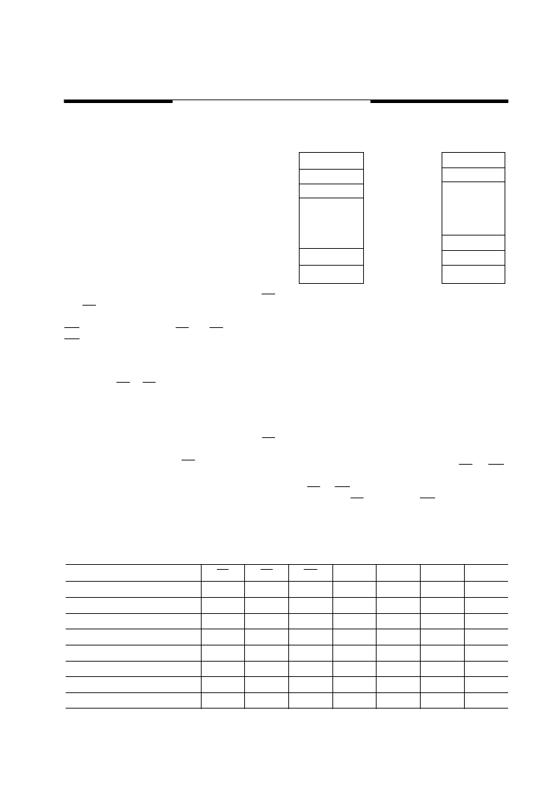
8KB Boot Block
512
512
512
512
512
512
512
512
8KB Boot Block
V29C51001T
V29C51001B
1FFFFH
1E000H
00000H
01FFFH
51001-13
00000H
8KB Boot Block = 16 Sectors
Table 1. Operation Modes Decoding
NOTES:
1.
2.
X = Don
’
t Care, V
IH
= HIGH, V
IL
= LOW. V
H
= 12.5V Max.
PD: The data at the byte address to be programmed.
Decoding Mode
CE
OE
WE
A
0
A
1
A
9
I/O
Read
V
IL
V
IL
V
IH
A
0
A
1
A
9
READ
Byte Write
V
IL
V
IH
V
IL
A
0
A
1
A
9
PD
Standby
V
IH
X
X
X
X
X
HIGH-Z
Autoselect Device ID
V
IL
V
IL
V
IH
V
IH
V
IL
V
H
CODE
Autoselect Manufacture ID
V
IL
V
IL
V
IH
V
IL
V
IL
V
H
CODE
Enabling Boot Block Protection Lock
V
IL
V
H
V
IL
X
X
V
H
X
Disabling Boot Block Protection Lock
V
H
V
H
V
IL
X
X
V
H
X
Output Disable
V
IL
V
IH
V
IH
X
X
X
HIGH-Z
相關(guān)PDF資料 |
PDF描述 |
|---|---|
| V29C31004B | 4 MEGABIT 524,288 x 8 BIT 3.3 VOLT CMOS FLASH MEMORY |
| V29C51000B | 512K Bit 5 Volt CMOS Flash Memory(512K位5V CMOS閃速存儲(chǔ)器) |
| V29C51000T-90P | 512K BIT 65,536 x 8 BIT 5 VOLT CMOS FLASH MEMORY |
| V29C51001B | 1 MEGA Bit 5 Volt CMOS Flash Memory(1M位5V CMOS閃速存儲(chǔ)器) |
| V29C51002B-55J | 2 MEGABIT 262,144 x 8 BIT 5 VOLT CMOS FLASH MEMORY |
相關(guān)代理商/技術(shù)參數(shù) |
參數(shù)描述 |
|---|---|
| V29C31001B-70T | 制造商:MOSEL 制造商全稱:MOSEL 功能描述:1 MEGABIT 131,072 x 8 BIT 5 VOLT CMOS FLASH MEMORY |
| V29C31001B-90J | 制造商:MOSEL 制造商全稱:MOSEL 功能描述:1 MEGABIT 131,072 x 8 BIT 5 VOLT CMOS FLASH MEMORY |
| V29C31001B-90P | 制造商:MOSEL 制造商全稱:MOSEL 功能描述:1 MEGABIT 131,072 x 8 BIT 5 VOLT CMOS FLASH MEMORY |
| V29C31001B-90T | 制造商:MOSEL 制造商全稱:MOSEL 功能描述:1 MEGABIT 131,072 x 8 BIT 5 VOLT CMOS FLASH MEMORY |
| V29C31001T-45J | 制造商:MOSEL 制造商全稱:MOSEL 功能描述:1 MEGABIT 131,072 x 8 BIT 5 VOLT CMOS FLASH MEMORY |
發(fā)布緊急采購(gòu),3分鐘左右您將得到回復(fù)。