- 您現(xiàn)在的位置:買賣IC網(wǎng) > PDF目錄384043 > UPD44324092F5-E50-EQ2-A (NEC Corp.) 36M-BIT DDRII SRAM 2-WORD BURST OPERATION PDF資料下載
參數(shù)資料
| 型號(hào): | UPD44324092F5-E50-EQ2-A |
| 廠商: | NEC Corp. |
| 元件分類: | DRAM |
| 英文描述: | 36M-BIT DDRII SRAM 2-WORD BURST OPERATION |
| 中文描述: | 36M條位SRAM的2條DDRII字爆發(fā)運(yùn)作 |
| 文件頁(yè)數(shù): | 25/40頁(yè) |
| 文件大?。?/td> | 361K |
| 代理商: | UPD44324092F5-E50-EQ2-A |
第1頁(yè)第2頁(yè)第3頁(yè)第4頁(yè)第5頁(yè)第6頁(yè)第7頁(yè)第8頁(yè)第9頁(yè)第10頁(yè)第11頁(yè)第12頁(yè)第13頁(yè)第14頁(yè)第15頁(yè)第16頁(yè)第17頁(yè)第18頁(yè)第19頁(yè)第20頁(yè)第21頁(yè)第22頁(yè)第23頁(yè)第24頁(yè)當(dāng)前第25頁(yè)第26頁(yè)第27頁(yè)第28頁(yè)第29頁(yè)第30頁(yè)第31頁(yè)第32頁(yè)第33頁(yè)第34頁(yè)第35頁(yè)第36頁(yè)第37頁(yè)第38頁(yè)第39頁(yè)第40頁(yè)
25
Data Sheet M16780EJ3V0DS
μ
PD44324082, 44324092, 44324182, 44324362
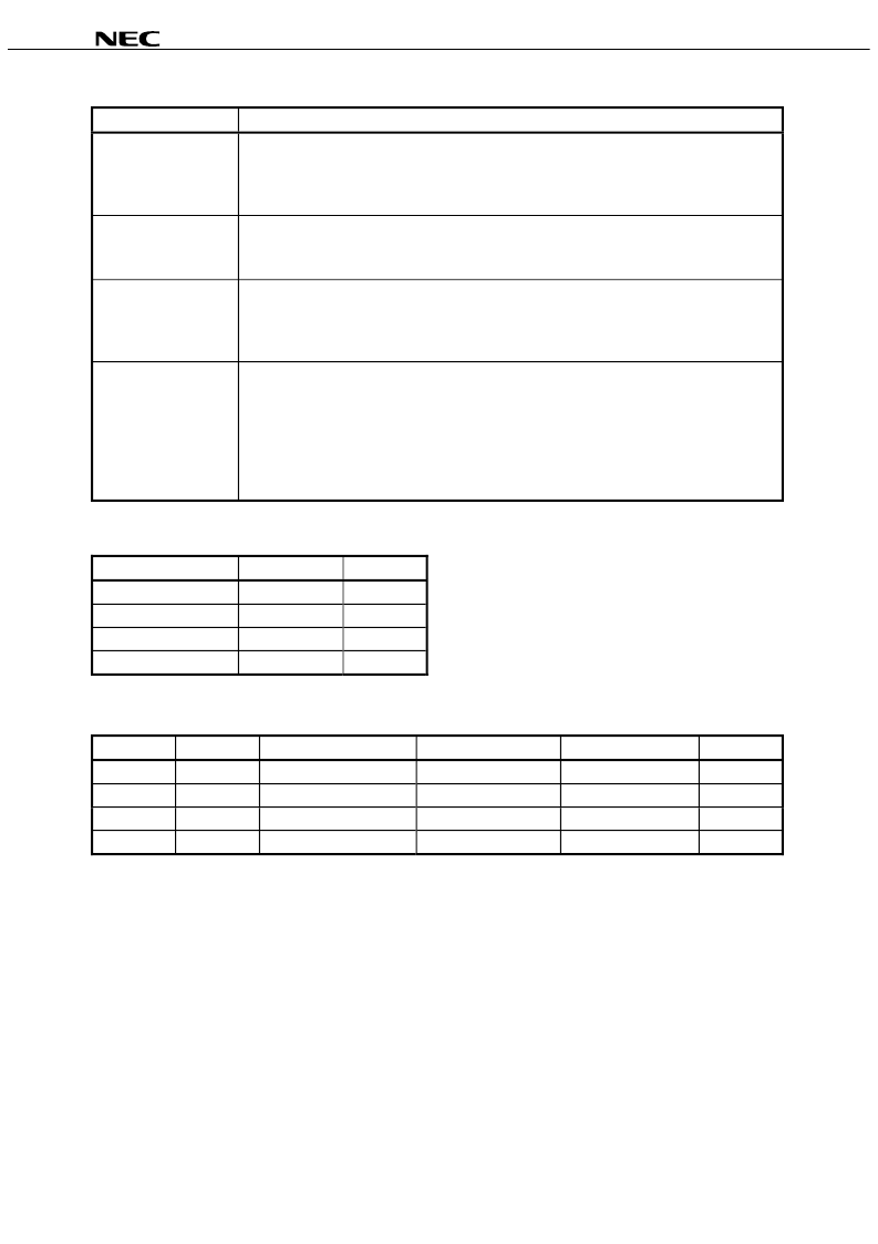
Scan Register Definition (1)
Register name
Description
Instruction register
The instruction register holds the instructions that are executed by the TAP controller when it is
moved into the run-test/idle or the various data register state. The register can be loaded when it is
placed between the TDI and TDO pins. The instruction register is automatically preloaded with the
IDCODE instruction at power-up whenever the controller is placed in test-logic-reset state.
Bypass register
The bypass register is a single bit register that can be placed between TDI and TDO. It allows serial
test data to be passed through the RAMs TAP to another device in the scan chain with as little delay
as possible.
ID register
The ID Register is a 32 bit register that is loaded with a device and vendor specific 32 bit code when
the controller is put in capture-DR state with the IDCODE command loaded in the instruction register.
The register is then placed between the TDI and TDO pins when the controller is moved into shift-DR
state.
Boundary register
The boundary register, under the control of the TAP controller, is loaded with the contents of the
RAMs I/O ring when the controller is in capture-DR state and then is placed between the TDI and
TDO pins when the controller is moved to shift-DR state. Several TAP instructions can be used to
activate the boundary register.
The Scan Exit Order tables describe which device bump connects to each boundary register
location. The first column defines the bit’s position in the boundary register. The second column is
the name of the input or I/O at the bump and the third column is the bump number.
Scan Register Definition (2)
Register name
Bit size
Unit
Instruction register
3
bit
Bypass register
1
bit
ID register
32
bit
Boundary register
109
bit
ID Register Definition
Part number
Organization ID [31:28] vendor revision no.
ID [27:12] part no.
ID [11:1] vendor ID no.
ID [0] fix bit
μ
PD44324082
4M x 8
XXXX
0000 0000 0011 1101
00000010000
1
μ
PD44324092
4M x 9
XXXX
0000 0000 0011 1110
00000010000
1
μ
PD44324182
2M x 18
XXXX
0000 0000 0011 1111
00000010000
1
μ
PD44324362
1M x 36
XXXX
0000 0000 0100 0000
00000010000
1
相關(guān)PDF資料 |
PDF描述 |
|---|---|
| UPD44324182F5-E37-EQ2 | 36M-BIT DDRII SRAM 2-WORD BURST OPERATION |
| UPD44324182F5-E37-EQ2-A | 36M-BIT DDRII SRAM 2-WORD BURST OPERATION |
| UPD44324182F5-E40-EQ2-A | 36M-BIT DDRII SRAM 2-WORD BURST OPERATION |
| UPD44324182F5-E50-EQ2-A | 36M-BIT DDRII SRAM 2-WORD BURST OPERATION |
| UPD44324362F5-E37-EQ2 | 36M-BIT DDRII SRAM 2-WORD BURST OPERATION |
相關(guān)代理商/技術(shù)參數(shù) |
參數(shù)描述 |
|---|---|
| UPD44324182BF5-E40-FQ1-A | 制造商:Renesas Electronics Corporation 功能描述:RENUPD44324182BF5-E40-FQ1-A 36M-BIT(2M-W |
| UPD44324185BF5-E40-FQ1 | 制造商:Renesas Electronics Corporation 功能描述:SRAM Chip Sync Dual 1.8V 36M-Bit 2M x 18 0.45ns 165-Pin BGA 制造商:Renesas Electronics Corporation 功能描述:36MB, DDRII SRAM - Trays 制造商:Renesas Electronics Corporation 功能描述:IC SRAM DDRII 36MBIT 165BGA |
| UPD44324362BF5-E40-FQ1 | 制造商:Renesas Electronics Corporation 功能描述:36MB, DDRII SRAM - Trays 制造商:Renesas Electronics Corporation 功能描述:IC SRAM DDRII 36MBIT 165BGA |
| UPD44324362BF5-E40-FQ1-A | 制造商:Renesas Electronics Corporation 功能描述:36MB, DDRII SRAM - Trays 制造商:Renesas Electronics Corporation 功能描述:IC SRAM DDRII 36MBIT 165BGA |
| UPD44324365BF5-E40-FQ1 | 制造商:Renesas Electronics Corporation 功能描述:36MB, DDRII SRAM - Trays 制造商:Renesas Electronics Corporation 功能描述:IC SRAM DDRII 36MBIT 165BGA |
發(fā)布緊急采購(gòu),3分鐘左右您將得到回復(fù)。