- 您現(xiàn)在的位置:買賣IC網(wǎng) > PDF目錄383981 > UPD44164082 (NEC Corp.) 18M-BIT DDRII SRAM 2-WORD BURST OPERATION PDF資料下載
參數(shù)資料
| 型號: | UPD44164082 |
| 廠商: | NEC Corp. |
| 英文描述: | 18M-BIT DDRII SRAM 2-WORD BURST OPERATION |
| 中文描述: | 1800萬位的SRAM 2條DDRII字爆發(fā)運作 |
| 文件頁數(shù): | 6/32頁 |
| 文件大小: | 275K |
| 代理商: | UPD44164082 |
第1頁第2頁第3頁第4頁第5頁當前第6頁第7頁第8頁第9頁第10頁第11頁第12頁第13頁第14頁第15頁第16頁第17頁第18頁第19頁第20頁第21頁第22頁第23頁第24頁第25頁第26頁第27頁第28頁第29頁第30頁第31頁第32頁
6
Data Sheet M15821EJ7V2DS
μ
PD44164082, 44164182, 44164362
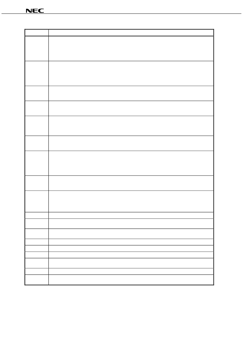
Pin Identification
Symbol
Description
A0
A
Synchronous Address Inputs: These inputs are registered and must meet the setup and hold times around the
rising edge of K. Balls 3A, 10A, and 2A are reserved for the next higher-order address inputs on future devices.
All transactions operate on a burst of two words (one clock period of bus activity). A0 is used as the lowest
order address bit permitting a random starting address within the burst operation. These inputs are ignored
when device is deselected.
Synchronous Data IOs: Input data must meet setup and hold times around the rising edges of K and /K. Output
data is synchronized to the respective C and /C data clocks or to K and /K if C and /C are tied to HIGH.
x8 device uses DQ0 to DQ7.
x18 device uses DQ0 to DQ17.
x36 device uses DQ0 to DQ35.
Synchronous Load: This input is brought LOW when a bus cycle sequence is to be defined. This definition
includes address and read/write direction. All transactions operate on a burst of 2 data (one clock period of bus
activity).
Synchronous Read/Write Input: When /LD is LOW, this input designates the access type (READ when R, /W is
HIGH, WRITE when R, /W is LOW) for the loaded address. R, /W must meet the setup and hold times around
the rising edge of K.
Synchronous Byte Writes (Nibble Writes on x8): When LOW these inputs cause their respective byte or nibble
to be registered and written during WRITE cycles. These signals must meet setup and hold times around the
rising edges of K and /K for each of the two rising edges comprising the WRITE cycle. See Pin Configurations
for signal to data relationships.
Input Clock: This input clock pair registers address and control inputs on the rising edge of K, and registers data
on the rising edge of K and the rising edge of /K. /K is ideally 180 degrees out of phase with K. All synchronous
inputs must meet setup and hold times around the clock rising edges.
Output Clock: This clock pair provides a user controlled means of tuning device output data. The rising edge of
/C is used as the output timing reference for first output data. The rising edge of C is used as the output
reference for second output data. Ideally, /C is 180 degrees out of phase with C. C and /C may be tied HIGH to
force the use of K and /K as the output reference clocks instead of having to provide C and /C clocks. If tied
HIGH, C and /C must remain HIGH and not be toggled during device operation.
Synchronous Echo Clock Outputs. The rising edges of these outputs are tightly matched to the synchronous
data outputs and can be used as a data valid indication. These signals run freely and do not stop when Q
tristates.
Output Impedance Matching Input: This input is used to tune the device outputs to the system data bus
impedance. DQ and CQ output impedance are set to 0.2 x RQ, where RQ is a resistor from this bump to
ground. This pin cannot be connected directly to GND or left unconnected. Also, in this product, there is no
function to minimize the output impedance by connecting ZQ directly to V
DD
Q.
DQ0 to DQxx
/LD
R, /W
/BWx
/NWx
K, /K
C, /C
CQ, /CQ
ZQ
/DLL
DLL Disable: When LOW, this input causes the DLL to be bypassed for stable low frequency operation.
TMS
TDI
TCK
IEEE 1149.1 Test Inputs: 1.8V I/O levels. These balls may be left Not Connected if the JTAG function is not
used in the circuit.
IEEE 1149.1 Clock Input: 1.8V I/O levels. This pin must be tied to V
SS
if the JTAG function is not used in the
circuit.
IEEE 1149.1 Test Output: 1.8V I/O level.
TDO
V
REF
HSTL Input Reference Voltage: Nominally V
DD
Q/2. Provides a reference voltage for the input buffers.
V
DD
Power Supply: 1.8V nominal. See DC Characteristics and Operating Conditions for range.
V
DD
Q
Power Supply: Isolated Output Buffer Supply. Nominally 1.5V. 1.8V is also permissible. See DC Characteristics
and Operating Conditions for range.
Power Supply: Ground
V
SS
NC
No Connect: These signals are internally connected and appear in the JTAG scan chain as the logic level
applied to the ball sites. These signals may be connected to ground to improve package heat dissipation.
相關(guān)PDF資料 |
PDF描述 |
|---|---|
| UPD44164182F5-E40-EQ1 | 18M-BIT DDRII SRAM 2-WORD BURST OPERATION |
| UPD44164082F5-E50-EQ1 | 18M-BIT DDRII SRAM 2-WORD BURST OPERATION |
| UPD44164182F5-E50-EQ1 | 18M-BIT DDRII SRAM 2-WORD BURST OPERATION |
| UPD44164362F5-E50-EQ1 | 18M-BIT DDRII SRAM 2-WORD BURST OPERATION |
| UPD44164082F5-E60-EQ1 | 18M-BIT DDRII SRAM 2-WORD BURST OPERATION |
相關(guān)代理商/技術(shù)參數(shù) |
參數(shù)描述 |
|---|---|
| UPD44164182AF5-E37Y-EQ2-A | 制造商:Renesas Electronics Corporation 功能描述:UPD44164182A Series 18 Mbit (1 M x 18 ) 270 MHz 0.3 ns DDRII SRAM - BGA-165 |
| UPD44164182F5-E50-EQ1 | 制造商:Renesas Electronics Corporation 功能描述:UPD44164182 Series 18 Mb (1 M x 18 ) 200 MHz 5 ns DDRII SRAM - BGA-165 |
| UPD44164362F5-E60-EQ1ES | 制造商:NEC Electronics Corporation 功能描述: |
| UPD44165092BF5-E40-EQ3-A | 制造商:Renesas Electronics Corporation 功能描述:2MX9, 2BURST, 250 MHZ QDRII SRAM - Trays |
| UPD44165094BF5-E40-EQ3-A | 制造商:Renesas Electronics Corporation 功能描述:SRAM Chip Sync Dual 1.8V 18M-Bit 2M x 9-Bit 0.45ns 165-Pin BGA |
發(fā)布緊急采購,3分鐘左右您將得到回復。