- 您現(xiàn)在的位置:買(mǎi)賣(mài)IC網(wǎng) > PDF目錄384041 > UPD16772AN (NEC Corp.) 480-OUTPUT TFT-LCD SOURCE DRIVER COMPATIBLE WITH 64-GRAY SCALES PDF資料下載
參數(shù)資料
| 型號(hào): | UPD16772AN |
| 廠商: | NEC Corp. |
| 英文描述: | 480-OUTPUT TFT-LCD SOURCE DRIVER COMPATIBLE WITH 64-GRAY SCALES |
| 中文描述: | 480輸出的TFT - LCD源驅(qū)動(dòng)程序完全兼容64灰度 |
| 文件頁(yè)數(shù): | 4/20頁(yè) |
| 文件大?。?/td> | 122K |
| 代理商: | UPD16772AN |
第1頁(yè)第2頁(yè)第3頁(yè)當(dāng)前第4頁(yè)第5頁(yè)第6頁(yè)第7頁(yè)第8頁(yè)第9頁(yè)第10頁(yè)第11頁(yè)第12頁(yè)第13頁(yè)第14頁(yè)第15頁(yè)第16頁(yè)第17頁(yè)第18頁(yè)第19頁(yè)第20頁(yè)
Data Sheet S14725EJ1V0DS00
4
μ
PD16772A
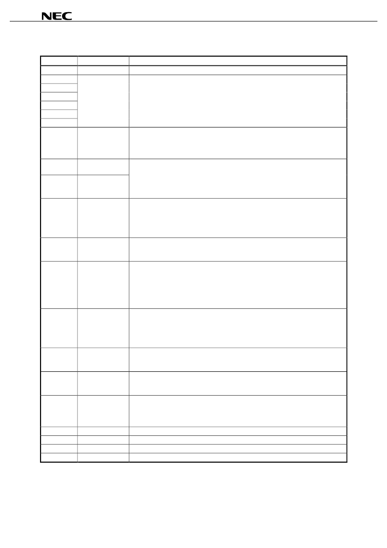
4. PIN FUNCTIONS
Pin Symbol
Pin Name
Description
S
1
to S
480
D
00
to D
05
D
10
to D
15
D
20
to D
25
D
30
to D
35
D
40
to D
45
D
50
to D
55
Driver output
Display data input
The D/A converted 64-gray-scale analog voltage is output.
The display data is input with a width of 36 bits, viz., the gray scale data (6 bits) by 6 dots (2
pixels).
D
X0
: LSB, D
X5
: MSB
R,/L
Shift direction control
input
These refer to the start pulse I/O pins when driver ICs are connected in cascade. The shift
directions of the shift registers are as follows.
R,/L = H: STHR input, S
1
→
S
480
, STHL output
R,/L = L: STHL input, S
480
→
S
1
, STHR output
These refer to the start pulse I/O pins when driver ICs are connected in cascade.
Fetching of display data starts when H is read at the rising edge of CLK.
R,/L = H (right shift): STHR input, STHL output
R,/L = L (left shift): STHL input, STHR output
The start pulse width (H level) for next-level drivers is 1CLK.
Refers to the shift register’s shift clock input. The display data is incorporated into the data
register at the rising edge. At the rising edge of the 80
th
clock after the start pulse input, the
start pulse output reaches the high level, thus becoming the start pulse of the next-level
driver. If 82 clock pulses are input after input of the start pulse, input of display data is halted
automatically. The contents of the shift register are cleared at the STB’s rising edge.
The contents of the data register are transferred to the latch circuit at the rising edge. And,
at the falling edge, the gray scale voltage is supplied to the driver. It is necessary to ensure
input of one pulse per horizontal period.
POL = L: The S
2n–1
output uses V
0
to V
4
as the reference supply. The S
2n
output uses V
5
to
V
9
as the reference supply.
POL = H: The S
2n–1
output uses V
5
to V
9
as the reference supply. The S
2n
output uses V
0
to
V
4
as the reference supply.
S
2n–1
indicates the odd output: and S
2n
indicates the even output. Input of the POL signal is
allowed the setup time(t
POL
-
STB
) with respect to STB’s rising edge.
Data inversion can invert when display data is loaded.
POL21/22 = H : Data inversion loads display data after inverting it.
POL21/22 = L : Data inversion does not invert input data.
POL21: D
00
to D
05
, D
10
to D
15
, D
20
to D
25
POL22: D
30
to D
35
, D
40
to D
45
, D
50
to D
55
The current consumption of V
DD2
is lowered by controlling the constant current source of the
output amplifier. This pin is pulled up to the V
DD1
power supply inside the IC. For details,
see
9. CURRENT CONSUMPTION REDUCTION FUNCTION.
This pin can be used to finely control the bias current inside the output amplifier.
When this fine-control function is not required, leave this pin open. For details, see
9. CURRENT CONSUMPTION REDUCTION FUNCTION.
Input the
γ
-corrected power supplies from outside by using operational amplifier. Make sure
to maintain the following relationships. During the gray scale voltage output, be sure to keep
the gray scale level power supply at a constant level.
V
DD2
0.1 V > V
0
> V
1
> V
2
> V
3
> V
4
> 0.5 V
DD2
> V
5
> V
6
> V
7
> V
8
> V
9
> V
SS2
+ 0.1 V
2.3 to 3.6 V
8.5 V
±
0.5 V
Grounding
Grounding
STHR
Right shift start pulse
input/output
Left shift start pulse
input/output
STHL
CLK
Shift clock input
STB
Latch input
POL
Polarity input
POL21,
POL22
Data inversion input
LPC
Low power control
input
Bcont
Bias control
V
0
to V
9
γ
-corrected power
supplies
V
DD1
V
DD2
V
SS1
V
SS2
Logic power supply
Driver power supply
Logic ground
Driver ground
相關(guān)PDF資料 |
PDF描述 |
|---|---|
| UPD16772 | 480-OUTPUT TFT-LCD SOURCE DRIVER COMPATIBLE WITH 64-GRAY SCALES |
| UPD16772N | 480-OUTPUT TFT-LCD SOURCE DRIVER COMPATIBLE WITH 64-GRAY SCALES |
| UPD168002GA-9EU | MONOLITHIC 6-CHANNEL H-BRIDGE DRIVER |
| UPD168002 | MONOLITHIC 6-CHANNEL H-BRIDGE DRIVER |
| UPD16804 | MONOLITHIC H BRIDGE DRIVER CIRCUIT |
相關(guān)代理商/技術(shù)參數(shù) |
參數(shù)描述 |
|---|---|
| UPD16772B | 制造商:未知廠家 制造商全稱(chēng):未知廠家 功能描述:UPD16772B Data Sheet | Data Sheet[07/2002] |
| UPD16772N | 制造商:NEC 制造商全稱(chēng):NEC 功能描述:480-OUTPUT TFT-LCD SOURCE DRIVER COMPATIBLE WITH 64-GRAY SCALES |
| UPD16780 | 制造商:NEC 制造商全稱(chēng):NEC 功能描述:288/300 OUTPUT TFT-LCD SOURCE DRIVER |
| UPD16780A | 制造商:未知廠家 制造商全稱(chēng):未知廠家 功能描述:UPD16780A Data Sheet | Data Sheet[11/2000] |
| UPD16780N | 制造商:NEC 制造商全稱(chēng):NEC 功能描述:288/300 OUTPUT TFT-LCD SOURCE DRIVER |
發(fā)布緊急采購(gòu),3分鐘左右您將得到回復(fù)。