- 您現(xiàn)在的位置:買賣IC網(wǎng) > PDF目錄384038 > UPA2700GR (NEC Corp.) SWITCHING N-CHANNEL POWER MOSFET PDF資料下載
參數(shù)資料
| 型號(hào): | UPA2700GR |
| 廠商: | NEC Corp. |
| 英文描述: | SWITCHING N-CHANNEL POWER MOSFET |
| 中文描述: | 開關(guān)N溝道功率MOSFET |
| 文件頁數(shù): | 1/8頁 |
| 文件大小: | 62K |
| 代理商: | UPA2700GR |
The information in this document is subject to change without notice. Before using this document, please
confirm that this is the latest version.
Not all devices/types available in every country. Please check with local NEC representative for
availability and additional information.
2002
MOS FIELD EFFECT TRANSISTOR
μ
PA2700GR
SWITCHING
N-CHANNEL POWER MOS FET
DATA SHEET
Document No. G15672EJ2V0DS00 (2nd edition)
Date Published May 2002 NS CP(K)
Printed in Japan
The mark
#
shows major revised points.
DESCRIPTION
The
μ
PA2700GR is N-Channel MOS Field Effect Transistor
designed for DC/DC converters and power management
applications of notebook computers.
FEATURES
Low on-state resistance
R
DS(on)1
= 5.3 m
MAX. (V
GS
= 10 V, I
D
= 9.0 A)
R
DS(on)2
= 7.3 m
MAX. (V
GS
= 4.5 V, I
D
= 9.0 A)
Low C
iss
: C
iss
= 2600 pF TYP. (V
DS
= 10 V, V
GS
= 0 V)
Small and surface mount package (Power SOP8)
ORDERING INFORMATION
PART NUMBER
PACKAGE
μ
PA2700GR
Power SOP8
ABSOLUTE MAXIMUM RATINGS (T
A
= 25°C, All terminals are connected.)
Drain to Source Voltage (V
GS
= 0 V)
V
DSS
30
V
Gate to Source Voltage (V
DS
= 0 V)
V
GSS
±
20
±
17
±
68
2.0
V
Drain Current (DC)
Drain Current (pulse)
Note1
Total Power Dissipation (T
A
= 25°C)
Note2
I
D(DC)
A
I
D(pulse)
A
P
T
W
Channel Temperature
T
ch
150
°C
Storage Temperature
Single Avalanche Current
Note3
Single Avalanche Energy
Note3
T
stg
–55 to + 150
°C
I
AS
17
A
E
AS
28.9
mJ
Notes 1.
PW
≤
10
μ
s, Duty Cycle
≤
1%
2.
Mounted on ceramic substrate of 1200 mm
2
x 2.2 mm
3.
Starting T
ch
= 25°C, V
DD
= 15 V, R
G
= 25
, L = 100
μ
H, V
GS
= 20
→
0 V
Remark
Strong electric field, when exposed to this device, can cause destruction of the gate oxide and ultimately
degrade the device operation. Steps must be taken to stop generation of static electricity as much as possible,
and quickly dissipate it once, when it has occurred.
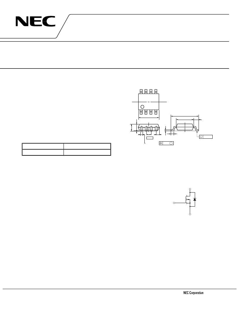
PACKAGE DRAWING (Unit: mm)
1.27
0.12 M
6.0 ±0.3
4.4
0.40
+0.10
0.78 MAX.
0
1
1
0.8
0.5 ±0.2
0
+
–
5.37 MAX.
0.10
1
4
8
5
1, 2, 3
4
5, 6, 7, 8 ; Drain
; Source
EQUIVALENT CIRCUIT
Source
Body
Diode
Gate
Drain
相關(guān)PDF資料 |
PDF描述 |
|---|---|
| UPA2700TP | SWITCHING N-CHANNEL POWER MOSFET |
| UPA2701GR | SWITCHING N-CHANNEL POWER MOSFET |
| UPA2701TP | WASHER FLAT NUB4 NYLON |
| UPA2702GR | NUT, HEX, 2-56 X STD THK, SST |
| UPA2702TP | SWITCHING N-CHANNEL POWER MOSFET |
相關(guān)代理商/技術(shù)參數(shù) |
參數(shù)描述 |
|---|---|
| UPA2700GR-E1-A | 制造商:Renesas Electronics Corporation 功能描述:Trans MOSFET N-CH 30V 17A 8-Pin Power SOP Cut Tape |
| UPA2700TP | 制造商:NEC 制造商全稱:NEC 功能描述:SWITCHING N-CHANNEL POWER MOSFET |
| UPA2700TP-E1-AZ | 制造商:Renesas Electronics 功能描述:Nch 30V 42A 5.3m@10V 8HSOP Cut Tape 制造商:Renesas 功能描述:Trans MOSFET N-CH 30V 17A 8-Pin Power HSOP T/R |
| UPA2701 | 制造商:未知廠家 制造商全稱:未知廠家 功能描述:UPA2701GR Data Sheet | Data Sheet[05/2002] |
| UPA2701GR | 制造商:NEC 制造商全稱:NEC 功能描述:SWITCHING N-CHANNEL POWER MOSFET |
發(fā)布緊急采購,3分鐘左右您將得到回復(fù)。