- 您現(xiàn)在的位置:買賣IC網(wǎng) > PDF目錄383974 > UPA1730G (NEC Corp.) SWITCHING P-CHANNEL POWER MOS FET INDUSTRIAL USE PDF資料下載
參數(shù)資料
| 型號: | UPA1730G |
| 廠商: | NEC Corp. |
| 英文描述: | SWITCHING P-CHANNEL POWER MOS FET INDUSTRIAL USE |
| 中文描述: | 開關(guān)P溝道功率MOS FET工業(yè)用 |
| 文件頁數(shù): | 1/8頁 |
| 文件大小: | 71K |
| 代理商: | UPA1730G |
The information in this document is subject to change without notice. Before using this document, please
confirm that this is the latest version.
Not all devices/types available in every country. Please check with local NEC representative for
availability and additional information.
1999
MOS FIELD EFFECT TRANSISTOR
μ
PA1730
SWITCHING
P-CHANNEL POWER MOS FET
INDUSTRIAL USE
DATA SHEET
Document No.
Date Published
Printed in Japan
G14284EJ1V0DS00 (1st edition)
November 1999 NS CP(K)
The mark
#
shows major revised points.
DESCRIPTION
The
μ
PA1730 is P-Channel MOS Field Effect Transis-
tor designed for power management applications of
notebook computers and Li-ion battery protection circuit.
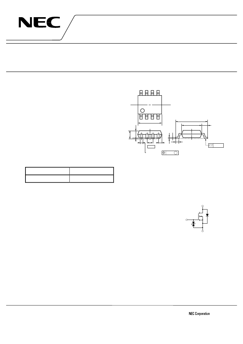
PACKAGE DRAWING (Unit : mm)
FEATURES
Low on-resistance
R
DS(on)1
= 9.5 m
MAX. (V
GS
= –10 V, I
D
= –6.5 A)
R
DS(on)2
= 13.5 m
MAX. (V
GS
= –4.5 V, I
D
= –6.5 A)
R
DS(on)3
= 15.0 m
MAX. (V
GS
= –4.0 V, I
D
= –6.5 A)
Low C
iss
: C
iss
= 3800 pF TYP.
Built-in G-S protection diode
Small and surface mount package (Power SOP8)
ORDERING INFORMATION
PART NUMBER
PACKAGE
μ
PA1730G
Power SOP8
ABSOLUTE MAXIMUM RATINGS (T
A
= 25°C, All terminals are connected.)
Drain to Source Voltage (V
GS
= 0 V)
V
DSS
–30
V
Gate to Source Voltage (V
DS
= 0 V)
V
GSS
#
20
#
13.0
#
52.0
2.2
V
Drain Current (DC)
Drain Current (pulse)
Note1
Total Power Dissipation (T
A
= 25°C)
Note2
I
D(DC)
A
I
D(pulse)
A
P
T
W
Channel Temperature
T
ch
150
°C
Storage Temperature
T
stg
–55 to +150
°C
Notes 1.
PW
≤
10
μ
s, Duty Cycle
≤
1 %
2.
Mounted on ceramic substrate of 1200 mm
2
x 2.2 mm
Remark
The diode connected between the gate and source of the transistor serves as a protector against ESD.
When this device actually used, an additional protection circuit is externally required if a voltage
exceeding the rated voltage may be applied to this device.
EQUIVALENT CIRCUIT
Source
Body
Diode
Gate
Protection
Diode
Gate
Drain
#
1.27
0.12 M
6.0 ±0.3
4.4
0.40
+0.10
0.78 MAX.
0
1
1
0.8
0.5 ±0.2
0
+
–
5.37 MAX.
0.10
1
4
8
5
1,2,3
4
5,6,7,8
; Source
; Gate
; Drain
相關(guān)PDF資料 |
PDF描述 |
|---|---|
| UPA1730TP | SWITCHING P-CHANNEL POWER MOSFET |
| UPA1731 | SWITCHING P-CHANNEL POWER MOS FET INDUSTRIAL USE |
| UPA1731G | SWITCHING P-CHANNEL POWER MOS FET INDUSTRIAL USE |
| UPA1740TP | SWITCHING N-CHANNEL POWER MOSFET |
| UPA1755 | Switching N-channel power MOS FET industrial use |
相關(guān)代理商/技術(shù)參數(shù) |
參數(shù)描述 |
|---|---|
| UPA1730TP | 制造商:NEC 制造商全稱:NEC 功能描述:SWITCHING P-CHANNEL POWER MOSFET |
| UPA1731 | 制造商:NEC 制造商全稱:NEC 功能描述:SWITCHING P-CHANNEL POWER MOS FET INDUSTRIAL USE |
| UPA1731G | 制造商:NEC 制造商全稱:NEC 功能描述:SWITCHING P-CHANNEL POWER MOS FET INDUSTRIAL USE |
| UPA1740 | 制造商:未知廠家 制造商全稱:未知廠家 功能描述:UPA1740TP Data Sheet | Data Sheet[05/2002] |
| UPA1740TP | 制造商:NEC 制造商全稱:NEC 功能描述:SWITCHING N-CHANNEL POWER MOSFET |
發(fā)布緊急采購,3分鐘左右您將得到回復(fù)。