- 您現(xiàn)在的位置:買賣IC網(wǎng) > PDF目錄98306 > TVP5154PNPRG4 (TEXAS INSTRUMENTS INC) COLOR SIGNAL DECODER, PQFP128 PDF資料下載
參數(shù)資料
| 型號(hào): | TVP5154PNPRG4 |
| 廠商: | TEXAS INSTRUMENTS INC |
| 元件分類: | 顏色信號(hào)轉(zhuǎn)換 |
| 英文描述: | COLOR SIGNAL DECODER, PQFP128 |
| 封裝: | PLASTIC, HTQFP-128 |
| 文件頁(yè)數(shù): | 67/77頁(yè) |
| 文件大小: | 795K |
| 代理商: | TVP5154PNPRG4 |
第1頁(yè)第2頁(yè)第3頁(yè)第4頁(yè)第5頁(yè)第6頁(yè)第7頁(yè)第8頁(yè)第9頁(yè)第10頁(yè)第11頁(yè)第12頁(yè)第13頁(yè)第14頁(yè)第15頁(yè)第16頁(yè)第17頁(yè)第18頁(yè)第19頁(yè)第20頁(yè)第21頁(yè)第22頁(yè)第23頁(yè)第24頁(yè)第25頁(yè)第26頁(yè)第27頁(yè)第28頁(yè)第29頁(yè)第30頁(yè)第31頁(yè)第32頁(yè)第33頁(yè)第34頁(yè)第35頁(yè)第36頁(yè)第37頁(yè)第38頁(yè)第39頁(yè)第40頁(yè)第41頁(yè)第42頁(yè)第43頁(yè)第44頁(yè)第45頁(yè)第46頁(yè)第47頁(yè)第48頁(yè)第49頁(yè)第50頁(yè)第51頁(yè)第52頁(yè)第53頁(yè)第54頁(yè)第55頁(yè)第56頁(yè)第57頁(yè)第58頁(yè)第59頁(yè)第60頁(yè)第61頁(yè)第62頁(yè)第63頁(yè)第64頁(yè)第65頁(yè)第66頁(yè)當(dāng)前第67頁(yè)第68頁(yè)第69頁(yè)第70頁(yè)第71頁(yè)第72頁(yè)第73頁(yè)第74頁(yè)第75頁(yè)第76頁(yè)第77頁(yè)
www.ti.com
4
Functional Description
4.1 Analog Front End
TVP5154
4-CHANNEL LOW-POWER PAL/NTSC/SECAM VIDEO DECODER
WITH INDEPENDENT SCALERS AND FAST LOCK
SLES163A – MARCH 2006 – REVISED JULY 2006
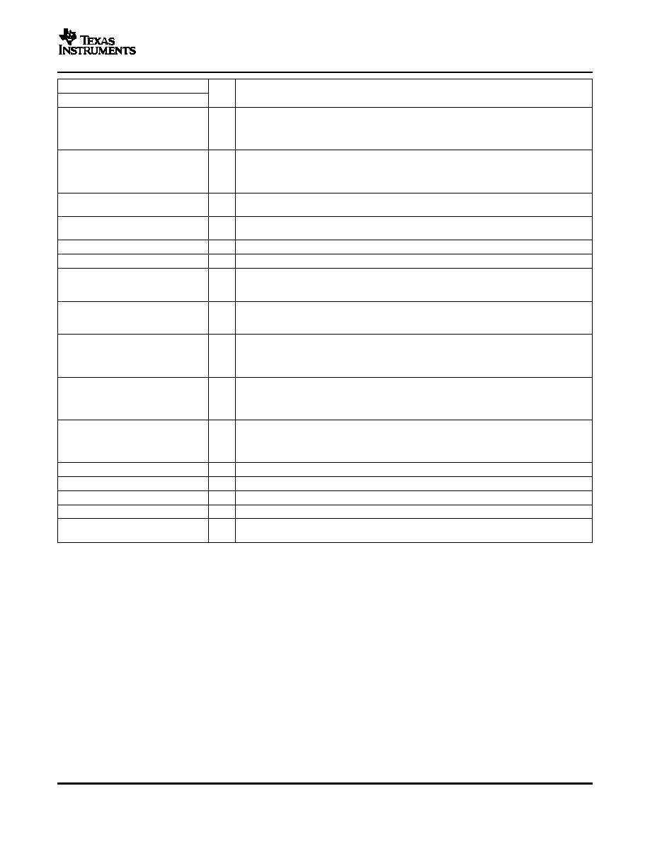
TERMINAL
I/O
DESCRIPTION
NAME
NO.
HSYNC1
100
O
Horizontal synchronization
HSYNC2
77
HSYNC3
58
HSYNC4
39
VSYNC1 /PALI1
95
O
1. VSYNC: Vertical synchronization
VSYNC2 /PALI2
76
2. PALI: PAL line indicator or horizontal lock indicator. For the PAL line indicator, a 1
VSYNC3 /PALI3
57
indicates a noninverted line, and a 0 indicates an inverted line.
VSYNC4 /PALI4
38
PDN
122
I
Power down (active low). A 0 on this pin puts the decoder in standby mode. PDN preserves
the value of the registers.
RESETB
121
I
Active-low reset. RESETB can be used only when PDN = 1. When RESETB is pulled low, it
resets all the registers and restarts the internal microprocessor.
SCL
120
I/O
I2C serial clock (open drain)
SDA
119
I/O
I2C serial data (open drain)
I2CA0
118
I
During power-on reset, this pin is sampled along with pin 117 (I2CA1) to determine the I2C
address the device is configured to. A 10-k
resistor should pull this either high (to IOVDD)
or low to select different I2C device addresses.
I2CA1
117
I
During power-on reset, this pin is sampled along with pin 118 (I2CA0) to determine the I2C
address the device is configured to. A 10-k
resistor should pull this either high (to IOVDD)
or low to select different I2C device addresses.
CLK1
103
O
Unscaled system data clock at either 27 MHz or 54 MHz
CLK2
84
CLK3
61
CLK4
42
SCLK1
104
O
Scaled system data clock at 27 MHz. This signal can be used to qualify scaled/unscaled
SCLK2
85
data when the unscaled system data clock is set to 54 MHz.
SCLK3
62
SCLK4
43
XIN/OSC
124
I
External clock reference. The user may connect XIN to an oscillator or to one terminal of a
XOUT
123
O
crystal oscillator. The user may connect XOUT to the other terminal of the crystal oscillator
or not connect XOUT at all. One single 14.31818-MHz crystal or oscillator is needed for
ITU-R BT.601 sampling, for all supported standards.
CH1_OUT[7:0]
105–112
O
Decoded ITU-R BT.656 output/YCbCr 4:2:2 output with discrete sync for channel 1
CH2_OUT[7:0]
86–93
O
Decoded ITU-R BT.656 output/YCbCr 4:2:2 output with discrete sync for channel 2
CH3_OUT[7:0]
67–74
O
Decoded ITU-R BT.656 output/YCbCr 4:2:2 output with discrete sync for channel 3
CH4_OUT[7:0]
48–55
O
Decoded ITU-R BT.656 output/YCbCr 4:2:2 output with discrete sync for channel 4
TMS
36
I
Test-mode select. This pin should be connected to digital ground for correct device
operation.
Each channel of the TVP5154 decoder has an analog input channel that accepts two video inputs, which
should be ac coupled through 0.1-
F capacitors. The decoder supports a maximum input voltage range of
0.75 V; therefore, an attenuation of one-half is needed for standard input signals with a peak-to-peak
variation of 1.5 V. The maximum parallel termination before the input to the device is 75
. Refer to
schematic at the end of this document for recommended configuration. The two analog input ports can be
connected as follows:
Two selectable composite video inputs or
One S-video input
An internal clamping circuit restores the ac-coupled video signal to a fixed dc level.
The programmable gain amplifier (PGA) and the automatic gain control (AGC) circuit work together to
ensure that the input signal is amplified or attenuated correctly, ensuring the proper input range for the
ADC.
Functional Description
7
相關(guān)PDF資料 |
PDF描述 |
|---|---|
| TVP5154PNPR | COLOR SIGNAL DECODER, PQFP128 |
| TVP5154PNP | COLOR SIGNAL DECODER, PQFP128 |
| TVP5157PNPR | COLOR SIGNAL DECODER, PQFP128 |
| TVP5157PNP | COLOR SIGNAL DECODER, PQFP128 |
| TVP5156PNPR | COLOR SIGNAL DECODER, PQFP128 |
相關(guān)代理商/技術(shù)參數(shù) |
參數(shù)描述 |
|---|---|
| TVP5156PNP | 功能描述:視頻 IC 4Ch NTSC/PAL Video Decoder RoHS:否 制造商:Fairchild Semiconductor 工作電源電壓:5 V 電源電流:80 mA 最大工作溫度:+ 85 C 封裝 / 箱體:TSSOP-28 封裝:Reel |
| TVP5156PNPR | 功能描述:視頻 IC 4Ch NTSC/PAL Video Decoder RoHS:否 制造商:Fairchild Semiconductor 工作電源電壓:5 V 電源電流:80 mA 最大工作溫度:+ 85 C 封裝 / 箱體:TSSOP-28 封裝:Reel |
| TVP5157PNP | 功能描述:視頻 IC 4Ch NTSC/PAL Video Decoder RoHS:否 制造商:Fairchild Semiconductor 工作電源電壓:5 V 電源電流:80 mA 最大工作溫度:+ 85 C 封裝 / 箱體:TSSOP-28 封裝:Reel |
| TVP5157PNPR | 功能描述:視頻 IC 4Ch NTSC/PAL Video Decoder RoHS:否 制造商:Fairchild Semiconductor 工作電源電壓:5 V 電源電流:80 mA 最大工作溫度:+ 85 C 封裝 / 箱體:TSSOP-28 封裝:Reel |
| TVP5158 | 制造商:TI 制造商全稱:Texas Instruments 功能描述:With Independent Scalers, Noise Reduction, Auto Contrast, and Flexible Output Formatter for Security and Other Multi-Channel Video Applications |
發(fā)布緊急采購(gòu),3分鐘左右您將得到回復(fù)。