- 您現(xiàn)在的位置:買賣IC網(wǎng) > PDF目錄98306 > TVP5154AIPNPR (TEXAS INSTRUMENTS INC) COLOR SIGNAL DECODER, PQFP128 PDF資料下載
參數(shù)資料
| 型號(hào): | TVP5154AIPNPR |
| 廠商: | TEXAS INSTRUMENTS INC |
| 元件分類: | 顏色信號(hào)轉(zhuǎn)換 |
| 英文描述: | COLOR SIGNAL DECODER, PQFP128 |
| 封裝: | PLASTIC, HTQFP-128 |
| 文件頁數(shù): | 64/92頁 |
| 文件大小: | 1089K |
| 代理商: | TVP5154AIPNPR |
第1頁第2頁第3頁第4頁第5頁第6頁第7頁第8頁第9頁第10頁第11頁第12頁第13頁第14頁第15頁第16頁第17頁第18頁第19頁第20頁第21頁第22頁第23頁第24頁第25頁第26頁第27頁第28頁第29頁第30頁第31頁第32頁第33頁第34頁第35頁第36頁第37頁第38頁第39頁第40頁第41頁第42頁第43頁第44頁第45頁第46頁第47頁第48頁第49頁第50頁第51頁第52頁第53頁第54頁第55頁第56頁第57頁第58頁第59頁第60頁第61頁第62頁第63頁當(dāng)前第64頁第65頁第66頁第67頁第68頁第69頁第70頁第71頁第72頁第73頁第74頁第75頁第76頁第77頁第78頁第79頁第80頁第81頁第82頁第83頁第84頁第85頁第86頁第87頁第88頁第89頁第90頁第91頁第92頁
www.ti.com
SLES214C – DECEMBER 2007 – REVISED SEPTEMBER 2010
7.2.68 Interrupt Configuration Register A
Address
C2h
Default
04h
7
6
5
4
3
2
1
0
Reserved
YCbCr enable (VDPOE)
Interrupt A
Interrupt polarity A
YCbCr enable (VDPOE):
0 = YCbCr pins are high impedance.
1 = YCbCr pins are active if other conditions are met (default).
Interrupt A (read only):
0 = Interrupt A is not active on the external pin (default).
1 = Interrupt A is active on the external pin.
Interrupt polarity A:
0 = Interrupt A is active low (default).
1 = Interrupt A is active high.
Interrupt configuration register A is used to configure the polarity of the external interrupt terminal. When
interrupt A is configured as active low, the terminal is driven low when active and high impedance when
inactive (open collector). Conversely, when the terminal is configured as active high, it is driven high when
active and driven low when inactive.
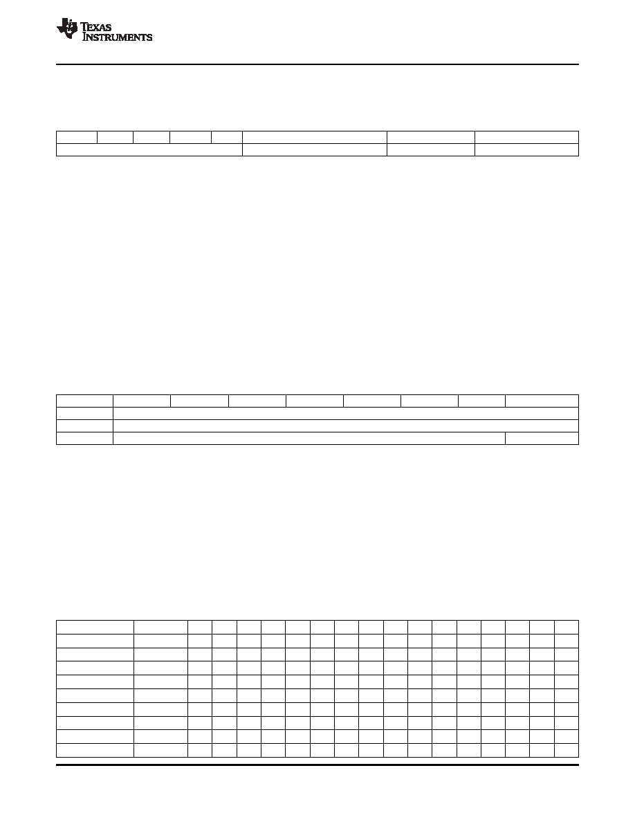
7.2.69 VDP Configuration RAM Register
Address
C3h
C4h
C5h
Default
B8h
1Fh
00h
Address
7
6
5
4
3
2
1
0
C3h
Configuration data
C4h
RAM address (7:0)
C5h
Reserved
RAM address 8
The configuration RAM data is provided to initialize the VDP with initial constants. The configuration RAM
is 512 bytes organized as 32 different configurations of 16 bytes each. The first 12 configurations are
defined for the current VBI standards. An additional two configurations can be used as a custom
programmed mode for unique standards, such as Gemstar.
Address C3h is used to read or write to the RAM. The RAM internal address counter is automatically
incremented with each transaction. Addresses C5h and C4h make up a 9-bit address to load the internal
address counter with a specific start address. This can be used to write a subset of the RAM for only
those standards of interest. Registers D0h–FBh must all be programmed with FFh before writing or
reading the configuration RAM. Full field mode (CFh) must be disabled as well.
The suggested RAM contents are shown in Table 7-11. All values are hexadecimal.
Table 7-11. VBI Configuration RAM for Signals With Pedestal
INDEX
ADDRESS
0
1
2
3
4
5
6
7
8
9
A
B
C
D
E
F
WST SECAM
000
AA
FF
E7
2E
20
A6
E4
B4
0E
0
7
0
10
0
WST SECAM
010
AA
FF
E7
2E
20
A6
E4
B4
0E
0
7
0
10
0
WST PAL B
020
AA
FF
27
2E
20
AB
A4
72
10
0
7
0
10
0
WST PAL B
030
AA
FF
27
2E
20
AB
A4
72
10
0
7
0
10
0
WST PAL C
040
AA
FF
E7
2E
20
22
A4
98
0D
0
10
0
WST PAL C
050
AA
FF
E7
2E
20
22
A4
98
0D
0
10
0
WST NTSC
060
AA
FF
27
2E
20
23
63
93
0D
0
10
0
WST NTSC
070
AA
FF
27
2E
20
23
63
93
0D
0
10
0
NABTS, NTSC
080
AA
FF
E7
2E
20
A2
63
93
0D
0
7
0
15
0
Copyright 2007–2010, Texas Instruments Incorporated
Internal Control Registers
67
Product Folder Link(s): TVP5154A
相關(guān)PDF資料 |
PDF描述 |
|---|---|
| TVP5154AIPNP | COLOR SIGNAL DECODER, PQFP128 |
| TVP5154APNPR | COLOR SIGNAL DECODER, PQFP128 |
| TVP5154APNP | COLOR SIGNAL DECODER, PQFP128 |
| TVP5154PNPG4 | COLOR SIGNAL DECODER, PQFP128 |
| TVP5154PNPRG4 | COLOR SIGNAL DECODER, PQFP128 |
相關(guān)代理商/技術(shù)參數(shù) |
參數(shù)描述 |
|---|---|
| TVP5154APNP | 功能描述:視頻 IC 4Ch Lo Pwr PAL/NTSC SECAM Vid Dec RoHS:否 制造商:Fairchild Semiconductor 工作電源電壓:5 V 電源電流:80 mA 最大工作溫度:+ 85 C 封裝 / 箱體:TSSOP-28 封裝:Reel |
| TVP5154APNPR | 功能描述:視頻 IC 4Ch Lo Pwr PAL/NTSC SECAM Vid Dec RoHS:否 制造商:Fairchild Semiconductor 工作電源電壓:5 V 電源電流:80 mA 最大工作溫度:+ 85 C 封裝 / 箱體:TSSOP-28 封裝:Reel |
| TVP5154EVM | 功能描述:視頻 IC 開發(fā)工具 TVP5154 Eval Mod RoHS:否 制造商:Texas Instruments 產(chǎn)品:Evaluation Boards 類型:YPbPr to RGBHV Converters 工具用于評(píng)估:LMH1251 工作電源電壓:5 V |
| TVP5154PNP | 功能描述:視頻 IC 4Ch Lo Pwr PAL/NTSC/ SECAM Video Decoder RoHS:否 制造商:Fairchild Semiconductor 工作電源電壓:5 V 電源電流:80 mA 最大工作溫度:+ 85 C 封裝 / 箱體:TSSOP-28 封裝:Reel |
| TVP5154PNP | 制造商:Texas Instruments 功能描述:4-Channel Video Decoder |
發(fā)布緊急采購,3分鐘左右您將得到回復(fù)。