- 您現(xiàn)在的位置:買賣IC網(wǎng) > Datasheet目錄57 > TSL210 (AMS-TAOS USA Inc)IC LINEAR SENSOR ARRAY 640X1 Datasheet資料下載
參數(shù)資料
| 型號: | TSL210 |
| 廠商: | AMS-TAOS USA Inc |
| 文件頁數(shù): | 6/13頁 |
| 文件大小: | 603K |
| 描述: | IC LINEAR SENSOR ARRAY 640X1 |
| 標準包裝: | 20 |
| 系列: | * |

TSL210
640 ?1 LINEAR SENSOR ARRAY
TAOS039D AUGUST 2011
5
The LUMENOLOGY r Company
r
r
Copyright E 2011, TAOS Inc.
www.taosinc.com
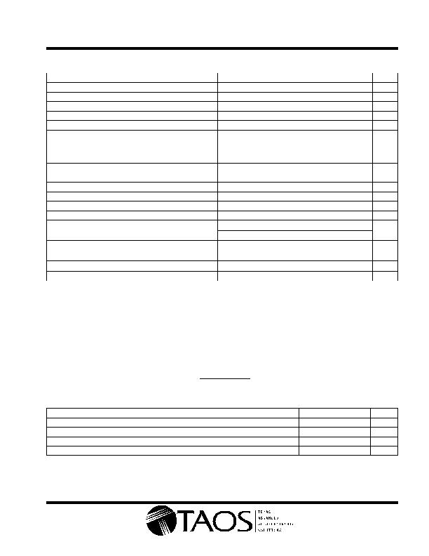
Electrical Characteristics at f
clock
= 200 kHz, V
DD
= 5 V, T
A
= 25?/SPAN>C, ?/SPAN>
p
= 640 nm, t
int
= 5 ms,
R
L
= 330 ?/SPAN>, E
e
= 18?/SPAN>W/cm
2
(unless otherwise noted) (see Note 3)
PARAMETER
TEST CONDITIONS
MIN
TYP
MAX
UNIT
V
OUT
Analog output voltage (white, average over 640 pixels)
See Note 2
1.6
2
2.4
V
V
DRK
Analog output voltage (dark, average over 640 pixels)
E
e
= 0
0
0.05
0.15
V
PRNU
Pixel response nonuniformity
See Note 4
?0
%
Nonlinearity of analog output voltage
See Note 5
?.4%
FS
Output noise voltage
See Note 6
1
mVrms
R
e
Responsivity
16
22
28
V/
(糐/
cm
2
)
SE
Saturation exposure
See Note 7
155
nJ/cm
2
V
SAT
Analog output saturation voltage
2.5
3.4
V
DSNU
Dark signal nonuniformity
All pixels, E
e
= 0, See Note 8
0.04
0.12
V
IL
Image lag
See Note 9
0.5
%
I
DD
Supply current
37
50
mA
I
IH
High-level input current
V
I
= V
DD
10
糀
I
IL
Low-level input current
V
I
= 0
10
糀
I
O
= 50 糀
4.5
4.95
V
OH
High-level output voltage, SO1 SO5
I
O
= 4 mA
4.6
V
I
O
= 50 糀
0.01
0.1
V
OL
Low-level output voltage, SO1 SO5
I
O
= 4 mA
0.4
V
C
i(SI)
Input capacitance, SI
20
pF
C
i(CLK)
Input capacitance, CLK
50
pF
NOTES: 2. The array is uniformly illuminated with a diffused LED source having a peak wavelength of 640 nm.
3. Clock duty cycle is assumed to be 50%.
4. PRNU is the maximum difference between the voltage from any single pixel and the average output voltage from all pixels of the
device under test when the array is uniformly illuminated.
5. Nonlinearity is defined as the maximum deviation from a best-fit straight line over the dark-to-white irradiance levels, as a percent
of analog output voltage (white).
6. RMS noise is the standard deviation of a single-pixel output under constant illumination as observed over a 5-second period.
7. Minimum saturation exposure is calculated using the minimum V
sat
, the maximum V
drk
, and the maximum R
e
.
8. DSNU is the difference between the maximum and minimum output voltage in the absence of illumination.
9. Image lag is a residual signal left in a pixel from a previous exposure. It is defined as a percent of white-level signal remaining after
a pixel is exposed to a white condition followed by a dark condition:
IL +
V
out (IL)
* V
drk
V
out (white)
* V
drk
100
Timing Requirements (see Figure 1 and Figure 2)
MIN
NOM
MAX
UNIT
t
su(SI)
Setup time, serial input (see Note 10)
20
ns
t
h(SI)
Hold time, serial input (see Note 10 and Note 11)
0
ns
t
w
Pulse duration, clock high or low
50
ns
t
r
, t
f
Input transition (rise and fall) time
0
500
ns
NOTES: 10. Input pulses have the following characteristics: t
r
= 6 ns, t
f
= 6 ns.
11. SI must go low before the rising edge of the next clock pulse.
相關(guān)PDF資料 |
PDF描述 |
|---|---|
| TSL230BRD-TR | IC LIGHT TO FREQUENCY CONV 8SOIC |
| TSL235RSM-LF | IC LIGHT TO FREQUENCY CONV 3SMD |
| TSL237SM-LF | IC LIGHT TO FREQUENCY CONV 3SMD |
| TSL237T | IC LIGHT TO FREQUENCY CONV 4-TMB |
| TSL238D-TR | IC LIGHT TO FREQUENCY CONV 8SOIC |
相關(guān)代理商/技術(shù)參數(shù) |
參數(shù)描述 |
|---|---|
| TSL213 | 制造商:Rochester Electronics LLC 功能描述:- Bulk |
| TSL213A | 制造商:Rochester Electronics LLC 功能描述:- Bulk |
| TSL214 | 制造商:Rochester Electronics LLC 功能描述:- Bulk |
| TSL215 | 制造商:TI 制造商全稱:Texas Instruments 功能描述:128 】 1 INTEGRATED OPTO SENSOR |
| TSL216 | 制造商:未知廠家 制造商全稱:未知廠家 功能描述:Optoelectronic |
發(fā)布緊急采購,3分鐘左右您將得到回復(fù)。