- 您現(xiàn)在的位置:買賣IC網(wǎng) > PDF目錄383966 > TS83C51RB2-LCE (International Rectifier) High Performance 8-bit Microcontroller PDF資料下載
參數(shù)資料
| 型號(hào): | TS83C51RB2-LCE |
| 廠商: | International Rectifier |
| 英文描述: | High Performance 8-bit Microcontroller |
| 中文描述: | 高性能8位微控制器 |
| 文件頁(yè)數(shù): | 56/85頁(yè) |
| 文件大?。?/td> | 762K |
| 代理商: | TS83C51RB2-LCE |
第1頁(yè)第2頁(yè)第3頁(yè)第4頁(yè)第5頁(yè)第6頁(yè)第7頁(yè)第8頁(yè)第9頁(yè)第10頁(yè)第11頁(yè)第12頁(yè)第13頁(yè)第14頁(yè)第15頁(yè)第16頁(yè)第17頁(yè)第18頁(yè)第19頁(yè)第20頁(yè)第21頁(yè)第22頁(yè)第23頁(yè)第24頁(yè)第25頁(yè)第26頁(yè)第27頁(yè)第28頁(yè)第29頁(yè)第30頁(yè)第31頁(yè)第32頁(yè)第33頁(yè)第34頁(yè)第35頁(yè)第36頁(yè)第37頁(yè)第38頁(yè)第39頁(yè)第40頁(yè)第41頁(yè)第42頁(yè)第43頁(yè)第44頁(yè)第45頁(yè)第46頁(yè)第47頁(yè)第48頁(yè)第49頁(yè)第50頁(yè)第51頁(yè)第52頁(yè)第53頁(yè)第54頁(yè)第55頁(yè)當(dāng)前第56頁(yè)第57頁(yè)第58頁(yè)第59頁(yè)第60頁(yè)第61頁(yè)第62頁(yè)第63頁(yè)第64頁(yè)第65頁(yè)第66頁(yè)第67頁(yè)第68頁(yè)第69頁(yè)第70頁(yè)第71頁(yè)第72頁(yè)第73頁(yè)第74頁(yè)第75頁(yè)第76頁(yè)第77頁(yè)第78頁(yè)第79頁(yè)第80頁(yè)第81頁(yè)第82頁(yè)第83頁(yè)第84頁(yè)第85頁(yè)
56
4188E–8051–08/06
AT/TS8xC51Rx2
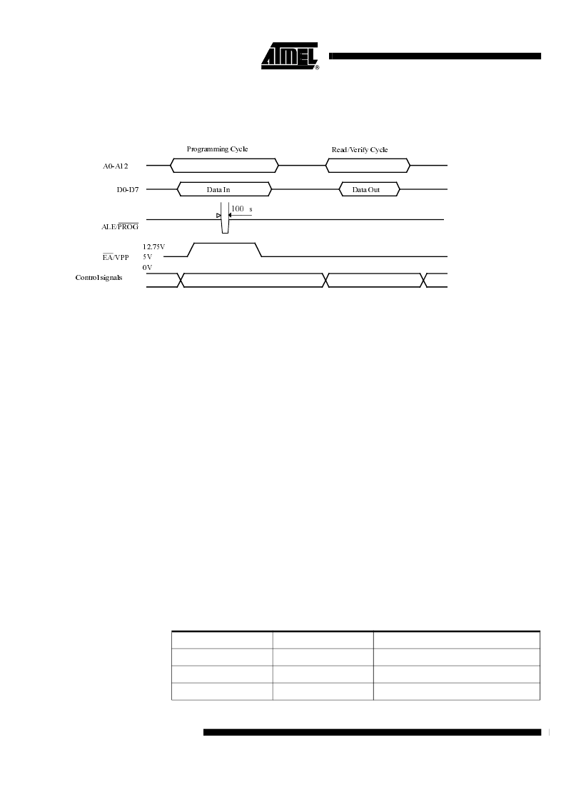
The encryption array cannot be directly verified. Verification of the encryption array is done by
observing that the code array is well encrypted.
Figure 9-2.
Programming and Verification Signal’s Waveform
9.4
EPROM Erasure (Windowed Packages Only)
Erasing the EPROM erases the code array, the encryption array and the lock bits returning the
parts to full functionality.
Erasure leaves all the EPROM cells in a 1’s state (FF).
9.4.1
Erasure Characteristics
The recommended erasure procedure is exposure to ultraviolet light (at 2537 ) to an integrated
dose at least 15 W-sec/cm
2
. Exposing the EPROM to an ultraviolet lamp of 12,000
μ
W/cm
2
rat-
ing for 30 minutes, at a distance of about 25 mm, should be sufficient. An exposure of 1 hour is
recommended with most of standard erasers.
Erasure of the EPROM begins to occur when the chip is exposed to light with wavelength
shorter than approximately 4,000 . Since sunlight and fluorescent lighting have wavelengths in
this range, exposure to these light sources over an extended time (about 1 week in sunlight, or 3
years in room-level fluorescent lighting) could cause inadvertent erasure. If an application sub-
jects the device to this type of exposure, it is suggested that an opaque label be placed over the
window.
10. Signature Bytes
The
TS83/87C51RB2/RC2/RD2
has four signature bytes in location 30h, 31h, 60h and 61h. To
read these bytes follow the procedure for EPROM verify but activate the control lines provided in
Table 31. for Read Signature Bytes. Table 10-1. shows the content of the signature byte for the
TS87C51RB2/RC2/RD2.
Table 10-1.
Signature Bytes Content
Control signals
Data In
ALE/PROG
A0-A12
Programming Cycle
100
μ
s
D0-D7
EA/VPP
Data Out
Read/Verify Cycle
12.75V
5V
0V
Location
Contents
Comment
30h
58h
Manufacturer Code: Atmel
31h
57h
Family Code: C51 X2
60h
7Ch
Product name: TS83C51RD2
相關(guān)PDF資料 |
PDF描述 |
|---|---|
| TS83C51RB2-LIB | High Performance 8-bit Microcontroller |
| TS83C51RB2-LIE | High Performance 8-bit Microcontroller |
| TS83C51RB2-MCB | High Performance 8-bit Microcontroller |
| TS83C51RB2-MCE | High Performance 8-bit Microcontroller |
| TS83C51RB2-MIB | High Performance 8-bit Microcontroller |
相關(guān)代理商/技術(shù)參數(shù) |
參數(shù)描述 |
|---|---|
| TS83C51RB2-LCEB | 制造商:未知廠家 制造商全稱:未知廠家 功能描述:8-Bit Microcontroller |
| TS83C51RB2-LCED | 制造商:未知廠家 制造商全稱:未知廠家 功能描述:8-Bit Microcontroller |
| TS83C51RB2-LIA | 制造商:未知廠家 制造商全稱:未知廠家 功能描述:8-Bit Microcontroller |
| TS83C51RB2-LIB | 制造商:ATMEL 制造商全稱:ATMEL Corporation 功能描述:High Performance 8-bit Microcontroller |
| TS83C51RB2-LIBR | 制造商:未知廠家 制造商全稱:未知廠家 功能描述:8-Bit Microcontroller |
發(fā)布緊急采購(gòu),3分鐘左右您將得到回復(fù)。