- 您現(xiàn)在的位置:買賣IC網(wǎng) > PDF目錄383966 > TS80C51RD2-LIE (International Rectifier) High Performance 8-bit Microcontroller PDF資料下載
參數(shù)資料
| 型號: | TS80C51RD2-LIE |
| 廠商: | International Rectifier |
| 英文描述: | High Performance 8-bit Microcontroller |
| 中文描述: | 高性能8位微控制器 |
| 文件頁數(shù): | 61/85頁 |
| 文件大小: | 762K |
| 代理商: | TS80C51RD2-LIE |
第1頁第2頁第3頁第4頁第5頁第6頁第7頁第8頁第9頁第10頁第11頁第12頁第13頁第14頁第15頁第16頁第17頁第18頁第19頁第20頁第21頁第22頁第23頁第24頁第25頁第26頁第27頁第28頁第29頁第30頁第31頁第32頁第33頁第34頁第35頁第36頁第37頁第38頁第39頁第40頁第41頁第42頁第43頁第44頁第45頁第46頁第47頁第48頁第49頁第50頁第51頁第52頁第53頁第54頁第55頁第56頁第57頁第58頁第59頁第60頁當前第61頁第62頁第63頁第64頁第65頁第66頁第67頁第68頁第69頁第70頁第71頁第72頁第73頁第74頁第75頁第76頁第77頁第78頁第79頁第80頁第81頁第82頁第83頁第84頁第85頁
61
4188E–8051–08/06
AT/TS8xC51Rx2
4. Capacitance loading on Ports 0 and 2 may cause spurious noise pulses to be superimposed on the V
OL
s of ALE and Ports 1
and 3. The noise is due to external bus capacitance discharging into the Port 0 and Port 2 pins when these pins make 1 to 0
transitions during bus operation. In the worst cases (capacitive loading 100pF), the noise pulse on the ALE line may exceed
0.45V with maxi V
OL
peak 0.6V. A Schmitt Trigger use is not necessary.
5. Typicals are based on a limited number of samples and are not guaranteed. The values listed are at room temperature and
5V.
6. Under steady state (non-transient) conditions, I
OL
must be externally limited as follows:
Maximum I
OL
per port pin: 10 mA
Maximum I
OL
per 8-bit port:
Port 0: 26 mA
Ports 1, 2, 3 and 4 and 5 when available: 15 mA
Maximum total I
OL
for all output pins: 71 mA
If I
OL
exceeds the test condition, V
OL
may exceed the related specification. Pins are not guaranteed to sink current greater
than the listed test conditions.
7. For other values, please contact your sales office.
8. Operating I
CC
is measured with all output pins disconnected; XTAL1 driven with T
CLCH
, T
CHCL
= 5 ns (see Figure 11-5.), V
IL
=
V
SS
+ 0.5 V,
V
IH
= V
CC
- 0.5V; XTAL2 N.C.; EA = Port 0 = V
CC
; RST = V
SS
. The internal ROM runs the code 80 FE (label: SJMP label). I
CC
would be slightly higher if a crystal oscillator is used. Measurements are made with OTP products when possible, which is
the worst case.
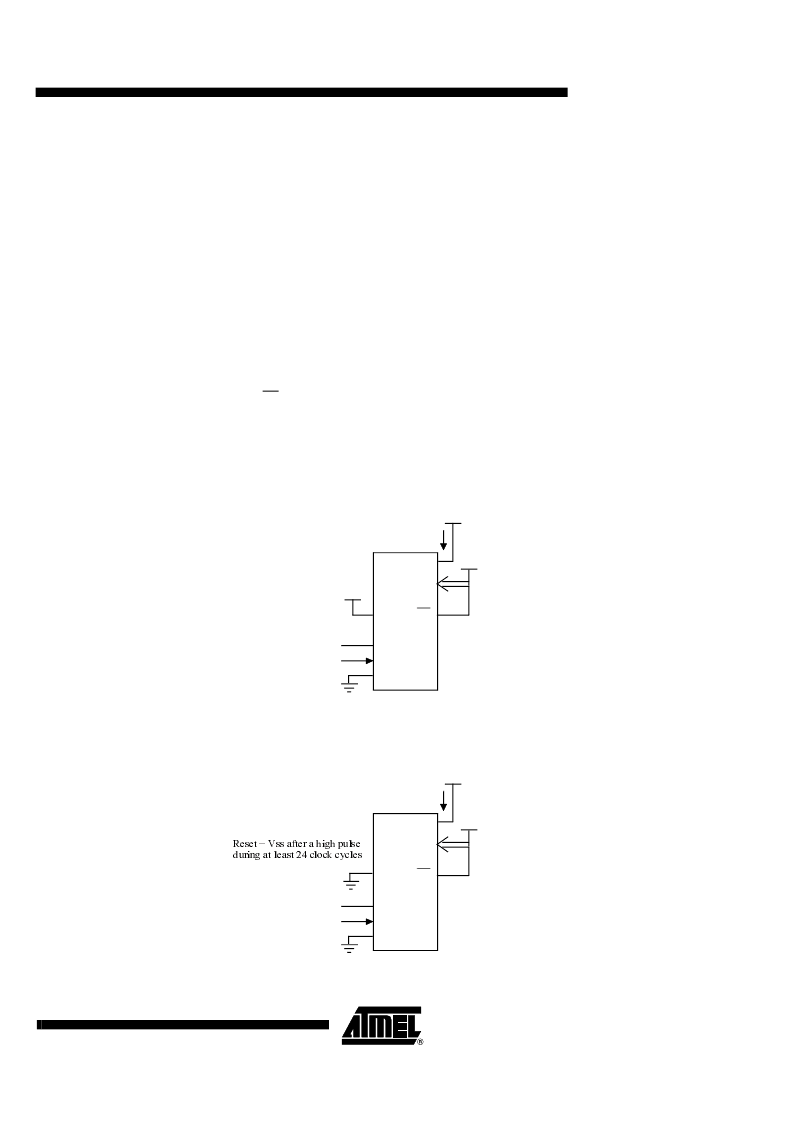
Figure 11-1.
I
CC
Test Condition, under reset
Figure 11-2.
Operating I
CC
Test Condition
EA
V
CC
V
CC
I
CC
(NC)
CLOCK
SIGNAL
V
CC
All other pins are disconnected.
RST
XTAL2
XTAL1
V
SS
V
CC
P0
EA
V
CC
V
CC
I
CC
(NC)
CLOCK
SIGNAL
All other pins are disconnected.
RST
XTAL2
XTAL1
V
SS
V
CC
P0
Reset = Vss after a high pulse
during at least 24 clock cycles
相關PDF資料 |
PDF描述 |
|---|---|
| TS80C51RD2-MCA | High Performance 8-bit Microcontroller |
| TS80C51RD2-MCB | High Performance 8-bit Microcontroller |
| TS80C51RD2-MCE | High Performance 8-bit Microcontroller |
| TS80C51RD2-MIA | High Performance 8-bit Microcontroller |
| TS80C51RD2-MIB | High Performance 8-bit Microcontroller |
相關代理商/技術參數(shù) |
參數(shù)描述 |
|---|---|
| TS80C51RD2-LIEB | 制造商:未知廠家 制造商全稱:未知廠家 功能描述:8-Bit Microcontroller |
| TS80C51RD2-LIED | 制造商:未知廠家 制造商全稱:未知廠家 功能描述:8-Bit Microcontroller |
| TS80C51RD2-LIER | 制造商:未知廠家 制造商全稱:未知廠家 功能描述:Microcontroller |
| TS80C51RD2-LIL | 制造商:ATMEL 制造商全稱:ATMEL Corporation 功能描述:High Performance 8-bit Microcontroller |
| TS80C51RD2-LILB | 制造商:未知廠家 制造商全稱:未知廠家 功能描述:8-Bit Microcontroller |
發(fā)布緊急采購,3分鐘左右您將得到回復。