- 您現(xiàn)在的位置:買賣IC網(wǎng) > PDF目錄300033 > TMP86FS64FG 8-BIT, FLASH, 16 MHz, MICROCONTROLLER, PQFP100 PDF資料下載
參數(shù)資料
| 型號: | TMP86FS64FG |
| 元件分類: | 微控制器/微處理器 |
| 英文描述: | 8-BIT, FLASH, 16 MHz, MICROCONTROLLER, PQFP100 |
| 封裝: | 20 X 14 MM, 0.65 MM PITCH, LEAD FREE, PLASTIC, QFP-100 |
| 文件頁數(shù): | 77/253頁 |
| 文件大小: | 1801K |
| 代理商: | TMP86FS64FG |
第1頁第2頁第3頁第4頁第5頁第6頁第7頁第8頁第9頁第10頁第11頁第12頁第13頁第14頁第15頁第16頁第17頁第18頁第19頁第20頁第21頁第22頁第23頁第24頁第25頁第26頁第27頁第28頁第29頁第30頁第31頁第32頁第33頁第34頁第35頁第36頁第37頁第38頁第39頁第40頁第41頁第42頁第43頁第44頁第45頁第46頁第47頁第48頁第49頁第50頁第51頁第52頁第53頁第54頁第55頁第56頁第57頁第58頁第59頁第60頁第61頁第62頁第63頁第64頁第65頁第66頁第67頁第68頁第69頁第70頁第71頁第72頁第73頁第74頁第75頁第76頁當(dāng)前第77頁第78頁第79頁第80頁第81頁第82頁第83頁第84頁第85頁第86頁第87頁第88頁第89頁第90頁第91頁第92頁第93頁第94頁第95頁第96頁第97頁第98頁第99頁第100頁第101頁第102頁第103頁第104頁第105頁第106頁第107頁第108頁第109頁第110頁第111頁第112頁第113頁第114頁第115頁第116頁第117頁第118頁第119頁第120頁第121頁第122頁第123頁第124頁第125頁第126頁第127頁第128頁第129頁第130頁第131頁第132頁第133頁第134頁第135頁第136頁第137頁第138頁第139頁第140頁第141頁第142頁第143頁第144頁第145頁第146頁第147頁第148頁第149頁第150頁第151頁第152頁第153頁第154頁第155頁第156頁第157頁第158頁第159頁第160頁第161頁第162頁第163頁第164頁第165頁第166頁第167頁第168頁第169頁第170頁第171頁第172頁第173頁第174頁第175頁第176頁第177頁第178頁第179頁第180頁第181頁第182頁第183頁第184頁第185頁第186頁第187頁第188頁第189頁第190頁第191頁第192頁第193頁第194頁第195頁第196頁第197頁第198頁第199頁第200頁第201頁第202頁第203頁第204頁第205頁第206頁第207頁第208頁第209頁第210頁第211頁第212頁第213頁第214頁第215頁第216頁第217頁第218頁第219頁第220頁第221頁第222頁第223頁第224頁第225頁第226頁第227頁第228頁第229頁第230頁第231頁第232頁第233頁第234頁第235頁第236頁第237頁第238頁第239頁第240頁第241頁第242頁第243頁第244頁第245頁第246頁第247頁第248頁第249頁第250頁第251頁第252頁第253頁
Page 155
TMP86FS64FG
When an external clock is used, the shift operation is synchronized with the external clock; therefore, the
previous data are read before the next data are transferred to the data buffer register. If the previous data have
not been read, the next data will not be transferred to the data buffer register and the receiving of any more data
will be canceled. When an external clock is used, the maximum transfer speed is determined by the delay
between the time when the interrupt request is generated and when the data received have been read.
The receiving is ended by clearing SIO1CR1<SIOS> to “0” or setting SIO1CR1<SIOINH> to “1” in buffer
full interrupt service program.
When SIO1CR1<SIOS> is cleared, the current data are transferred to the buffer. After SIO1CR1<SIOS>
cleared, the receiving is ended at the time that the final bit of the data has been received. That the receiving has
ended can be determined from the status of SIO1SR<SIOF>. SIO1SR<SIOF> is cleared to “0” when the
receiving is ended. After confirmed the receiving termination, the final receiving data is read. When
SIO1CR1<SIOINH> is set, the receiving is immediately ended and SIO1SR<SIOF> is cleared to “0”. (The
received data is ignored, and it is not required to be read out.)
If it is necessary to change the number of words in external clock operation, SIO1CR1<SIOS> should be
cleared to “0” then SIO1CR2<BUF> must be rewritten after confirming that SIO1SR<SIOF> has been cleared
to “0”. If it is necessary to change the number of words in internal clock, during automatic-wait operation
which occurs after completion of data receiving, SIO1CR2<BUF> must be rewritten before the received data is
read out.
Note:The buffer contents are lost when the transfer mode is switched. If it should become necessary to switch the
transfer mode, end receiving by clearing SIO1CR1<SIOS> to “0”, read the last data and then switch the trans-
fer mode.
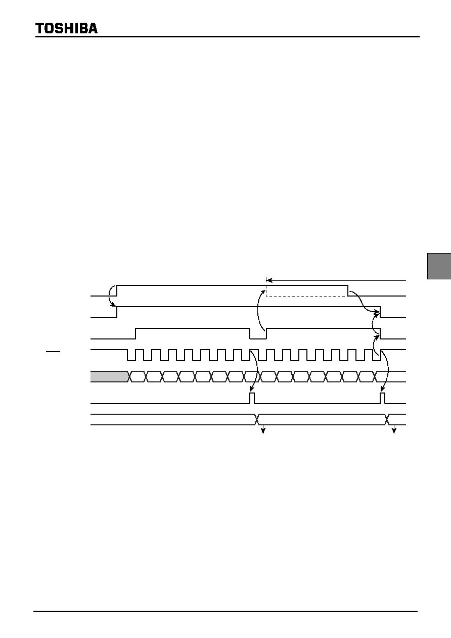
Figure 15-10 Receive Mode (Example: 8bit, 1word transfer, Internal clock)
15.6.3 8-bit transfer / receive mode
After setting the SIO control register to the 8-bit transmit/receive mode, write the data to be transmitted first
to the data buffer registers (DBR). After that, enable the transmit/receive by setting SIO1CR1<SIOS> to “1”.
When transmitting, the data are output from the SO1 pin at leading edges of the serial clock. When receiving,
the data are input to the SI1 pin at the trailing edges of the serial clock. When the all receive is enabled, 8-bit
data are transferred from the shift register to the data buffer register. An INTSIO1 interrupt is generated when
the number of data words specified with the SIO1CR2<BUF> has been transferred. Usually, read the receive
data from the buffer register in the interrupt service. The data buffer register is used for both transmitting and
receiving; therefore, always write the data to be transmitted after reading the all received data.
When the internal clock is used, a wait is initiated until the received data are read and the next transfer data
are written. A wait will not be initiated if even one transfer data word has been written.
a1
a0
a2
a3
a4
a5
a6
a7
b0
b1
b2
b3
b4
b5
b6
b7
DBR
b
a
Clear SIOS
Read out
SCK1 pin
(Output)
SI1 pin
INTSIO1 Interrupt
SIO1CR1<SIOS>
SIO1SR<SIOF>
SIO1SR<SEF>
相關(guān)PDF資料 |
PDF描述 |
|---|---|
| TMP87P409N | 8-BIT, MROM, 8 MHz, MICROCONTROLLER, PDIP28 |
| TMP87P808NG | 8-BIT, OTPROM, 8 MHz, MICROCONTROLLER, PDIP28 |
| TMP87PM14FG | 8-BIT, OTPROM, 8 MHz, MICROCONTROLLER, PQFP64 |
| TMP88CM38AFG | 8-BIT, MROM, 24 MHz, MICROCONTROLLER, PQFP44 |
| TMP88CP76F | 8-BIT, MROM, 12.5 MHz, MICROCONTROLLER, PQFP80 |
相關(guān)代理商/技術(shù)參數(shù) |
參數(shù)描述 |
|---|---|
| TMP86FS64FG(TZ) | 功能描述:8位微控制器 -MCU 60K Flash MCU RoHS:否 制造商:Silicon Labs 核心:8051 處理器系列:C8051F39x 數(shù)據(jù)總線寬度:8 bit 最大時鐘頻率:50 MHz 程序存儲器大小:16 KB 數(shù)據(jù) RAM 大小:1 KB 片上 ADC:Yes 工作電源電壓:1.8 V to 3.6 V 工作溫度范圍:- 40 C to + 105 C 封裝 / 箱體:QFN-20 安裝風(fēng)格:SMD/SMT |
| TMP86P202MG | 制造商:TOSHIBA 制造商全稱:Toshiba Semiconductor 功能描述:8 Bit Microcontroller |
| TMP86P202P | 制造商:TOSHIBA 制造商全稱:Toshiba Semiconductor 功能描述:High performance, Low Cost 20 pin OTP TMP86P202P |
| TMP86P202PG | 制造商:TOSHIBA 制造商全稱:Toshiba Semiconductor 功能描述:8 Bit Microcontroller |
| TMP86P203MG | 制造商:TOSHIBA 制造商全稱:Toshiba Semiconductor 功能描述:8 Bit Microcontroller |
發(fā)布緊急采購,3分鐘左右您將得到回復(fù)。