- 您現(xiàn)在的位置:買賣IC網(wǎng) > PDF目錄384024 > TMP320C6205GHK200 (Texas Instruments, Inc.) FIXED-POINT DIGITAL SIGNAL PROCESSOR PDF資料下載
參數(shù)資料
| 型號(hào): | TMP320C6205GHK200 |
| 廠商: | Texas Instruments, Inc. |
| 元件分類: | 數(shù)字信號(hào)處理 |
| 英文描述: | FIXED-POINT DIGITAL SIGNAL PROCESSOR |
| 中文描述: | 定點(diǎn)數(shù)字信號(hào)處理器 |
| 文件頁(yè)數(shù): | 63/72頁(yè) |
| 文件大小: | 1143K |
| 代理商: | TMP320C6205GHK200 |
第1頁(yè)第2頁(yè)第3頁(yè)第4頁(yè)第5頁(yè)第6頁(yè)第7頁(yè)第8頁(yè)第9頁(yè)第10頁(yè)第11頁(yè)第12頁(yè)第13頁(yè)第14頁(yè)第15頁(yè)第16頁(yè)第17頁(yè)第18頁(yè)第19頁(yè)第20頁(yè)第21頁(yè)第22頁(yè)第23頁(yè)第24頁(yè)第25頁(yè)第26頁(yè)第27頁(yè)第28頁(yè)第29頁(yè)第30頁(yè)第31頁(yè)第32頁(yè)第33頁(yè)第34頁(yè)第35頁(yè)第36頁(yè)第37頁(yè)第38頁(yè)第39頁(yè)第40頁(yè)第41頁(yè)第42頁(yè)第43頁(yè)第44頁(yè)第45頁(yè)第46頁(yè)第47頁(yè)第48頁(yè)第49頁(yè)第50頁(yè)第51頁(yè)第52頁(yè)第53頁(yè)第54頁(yè)第55頁(yè)第56頁(yè)第57頁(yè)第58頁(yè)第59頁(yè)第60頁(yè)第61頁(yè)第62頁(yè)當(dāng)前第63頁(yè)第64頁(yè)第65頁(yè)第66頁(yè)第67頁(yè)第68頁(yè)第69頁(yè)第70頁(yè)第71頁(yè)第72頁(yè)
SPRS106G OCTOBER 1999 REVISED JULY 2006
63
POST OFFICE BOX 1443
HOUSTON, TEXAS 772511443
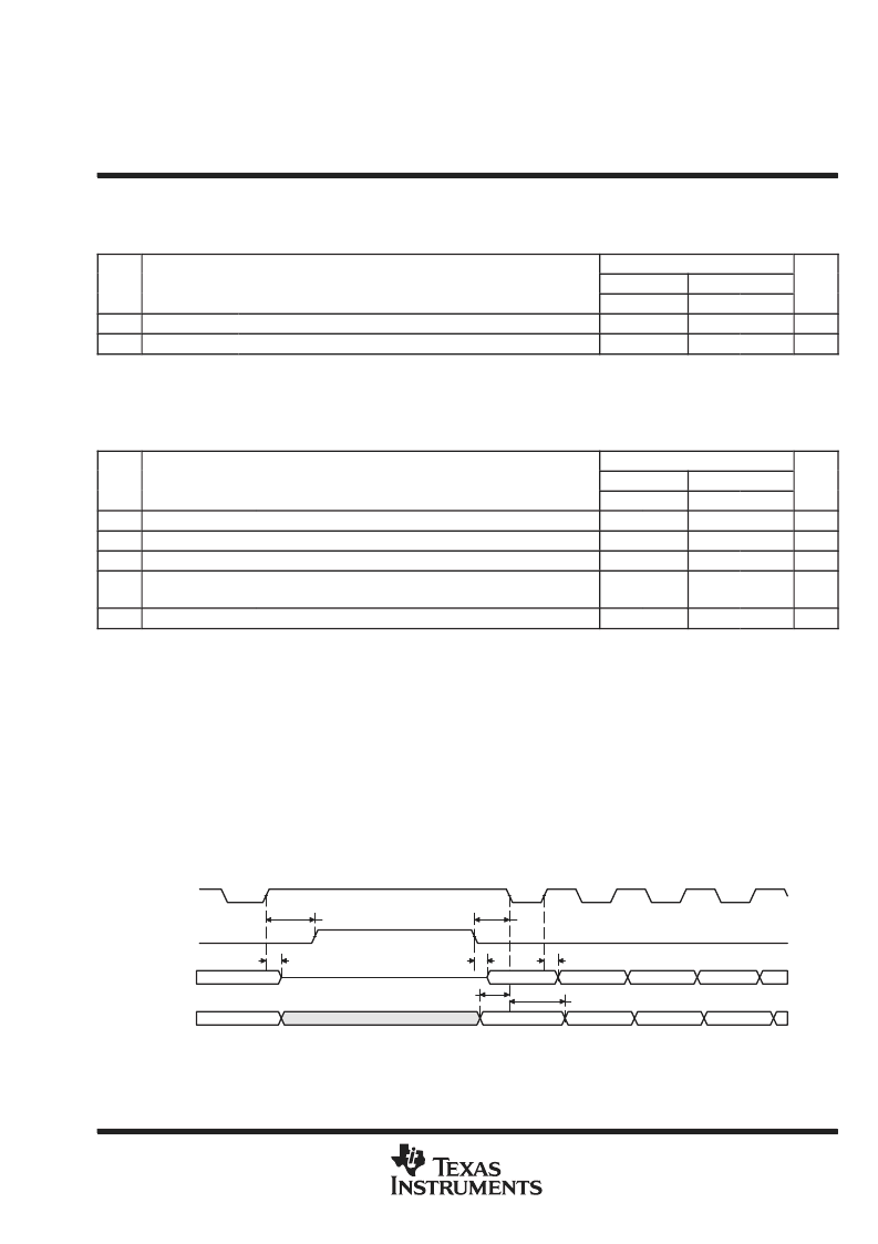
MULTICHANNEL BUFFERED SERIAL PORT TIMING (CONTINUED)
timing requirements for McBSP as SPI master or slave: CLKSTP = 11b, CLKXP = 1
(see Figure 38)
200
NO.
MASTER
MIN
SLAVE
MIN
UNIT
MAX
MAX
4
tsu(DRV-CKXL)
th(CKXL-DRV)
Setup time, DR valid before CLKX low
12
2 3P
ns
5
Hold time, DR valid after CLKX low
4
5 + 6P
ns
P = 1/CPU clock frequency in ns. For example, when running parts at 200 MHz, use P = 5 ns.
For all SPI slave modes, CLKG is programmed as 1/2 of the CPU clock by setting CLKSM = CLKGDV = 1.
switching characteristics over recommended operating conditions for McBSP as SPI master or
slave: CLKSTP = 11b, CLKXP = 1
(see Figure 38)
200
NO.
PARAMETER
MASTER§
SLAVE
UNIT
MIN
MAX
MIN
MAX
1
th(CKXH-FXL)
td(FXL-CKXL)
td(CKXH-DXV)
Hold time, FSX low after CLKX high
Delay time, FSX low to CLKX low#
H 2
H + 3
ns
2
T 2
T + 1
ns
3
Delay time, CLKX high to DX valid
2
4
3P + 4
5P + 17
ns
6
tdis(CKXH-DXHZ)
Disable time, DX high impedance following last data bit from
CLKX high
2
4
3P + 3
5P + 17
ns
7
td(FXL-DXV)
Delay time, FSX low to DX valid
L 2
L + 4
2P + 2
4P + 17
ns
P = 1/CPU clock frequency in ns. For example, when running parts at 200 MHz, use P = 5 ns.
For all SPI slave modes, CLKG is programmed as 1/2 of the CPU clock by setting CLKSM = CLKGDV = 1.
§S =
sample rate generator input clock = P if CLKSM = 1 (P = 1/CPU clock frequency)
=
sample rate generator input clock = P_clks if CLKSM = 0 (P_clks = CLKS period)
T =
CLKX period = (1 + CLKGDV) * S
H =
CLKX high pulse width = (CLKGDV/2 + 1) * S if CLKGDV is even
= (CLKGDV + 1)/2 * S if CLKGDV is odd or zero
L =
CLKX low pulse width
= (CLKGDV/2) * S if CLKGDV is even
= (CLKGDV + 1)/2 * S if CLKGDV is odd or zero
FSRP = FSXP = 1. As a SPI master, FSX is inverted to provide active-low slave-enable output. As a slave, the active-low signal input on FSX
and FSR is inverted before being used internally.
CLKXM = FSXM = 1, CLKRM = FSRM = 0 for master McBSP
CLKXM = CLKRM = FSXM = FSRM = 0 for slave McBSP
#FSX should be low before the rising edge of clock to enable slave devices and then begin a SPI transfer at the rising edge of the master clock
(CLKX).
Bit 0
Bit(n-1)
(n-2)
(n-3)
(n-4)
Bit 0
Bit(n-1)
(n-2)
(n-3)
(n-4)
5
4
3
7
6
2
1
CLKX
FSX
DX
DR
Figure 38. McBSP Timing as SPI Master or Slave: CLKSTP = 11b, CLKXP = 1
相關(guān)PDF資料 |
PDF描述 |
|---|---|
| TMP320C6205GHKA200 | FIXED-POINT DIGITAL SIGNAL PROCESSOR |
| TMP320C6205ZHK200 | FIXED-POINT DIGITAL SIGNAL PROCESSOR |
| TMP320C6205ZHKA200 | FIXED-POINT DIGITAL SIGNAL PROCESSOR |
| TMX320DM6446ZWT | Digital Media System on-Chip |
| TN28F010-90 | 28F010 1024K (128K X 8) CMOS FLASH MEMORY |
相關(guān)代理商/技術(shù)參數(shù) |
參數(shù)描述 |
|---|---|
| TMP320C6205GHKA100 | 制造商:TI 制造商全稱:Texas Instruments 功能描述:FIXED-POINT DIGITAL SIGNAL PROCESSOR |
| TMP320C6205GHKA200 | 制造商:TI 制造商全稱:Texas Instruments 功能描述:FIXED-POINT DIGITAL SIGNAL PROCESSOR |
| TMP320C6205GJC100 | 制造商:TI 制造商全稱:Texas Instruments 功能描述:FIXED-POINT DIGITAL SIGNAL PROCESSOR |
| TMP320C6205GJC120 | 制造商:TI 制造商全稱:Texas Instruments 功能描述:FIXED-POINT DIGITAL SIGNAL PROCESSOR |
| TMP320C6205GJCA100 | 制造商:TI 制造商全稱:Texas Instruments 功能描述:FIXED-POINT DIGITAL SIGNAL PROCESSOR |
發(fā)布緊急采購(gòu),3分鐘左右您將得到回復(fù)。