- 您現(xiàn)在的位置:買賣IC網(wǎng) > PDF目錄383949 > TL16C552AMFN (Texas Instruments, Inc.) DUAL ASYNCHRONOUS COMMUNICATIONS ELEMENT WITH FIFO PDF資料下載
參數(shù)資料
| 型號: | TL16C552AMFN |
| 廠商: | Texas Instruments, Inc. |
| 英文描述: | DUAL ASYNCHRONOUS COMMUNICATIONS ELEMENT WITH FIFO |
| 中文描述: | 雙異步通信元帶有FIFO |
| 文件頁數(shù): | 32/39頁 |
| 文件大小: | 545K |
| 代理商: | TL16C552AMFN |
第1頁第2頁第3頁第4頁第5頁第6頁第7頁第8頁第9頁第10頁第11頁第12頁第13頁第14頁第15頁第16頁第17頁第18頁第19頁第20頁第21頁第22頁第23頁第24頁第25頁第26頁第27頁第28頁第29頁第30頁第31頁當(dāng)前第32頁第33頁第34頁第35頁第36頁第37頁第38頁第39頁
TL16C552A, TL16C552AM
DUAL ASYNCHRONOUS COMMUNICATIONS ELEMENT
WITH FIFO
SLLS189D – NOVEMBER 1994 – REVISED JANUARY 1999
32
POST OFFICE BOX 655303
DALLAS, TEXAS 75265
PRINCIPLES OF OPERATION
parallel port registers
The TL16C552A parallel port can connect the device to a Centronic-style printer interface. When chip select 2
(CS2) is low, the parallel port is selected. Table 12 shows the registers associated with this parallel port. The
read or write function of the register is controlled by the state of the read (IOR) and write (IOW) terminals as
shown. The read data register allows the microprocessor to read the information on the parallel bus.
The read status register allows the microprocessor to read the status of the printer in the six most significant
bits. The status bits are printer busy BSY, acknowledge (ACK) (a handshake function), paper empty (PE), printer
selected (SLCT), error (ERR), and printer interrupt (PRINT). The read control register allows the state of the
control lines to be read. The write control register sets the state of the control lines. They are direction (DIR),
interrupt enable (INT2 EN), select in (SLIN), initialize the printer (INIT), autofeed the paper (AFD), and strobe
(STB), which informs the printer of the presence of a valid byte on the parallel bus. The write data register allows
the microprocessor to write a byte to the parallel bus. The parallel port is completely compatible with the parallel
port implementation used in the IBM serial parallel adapter.
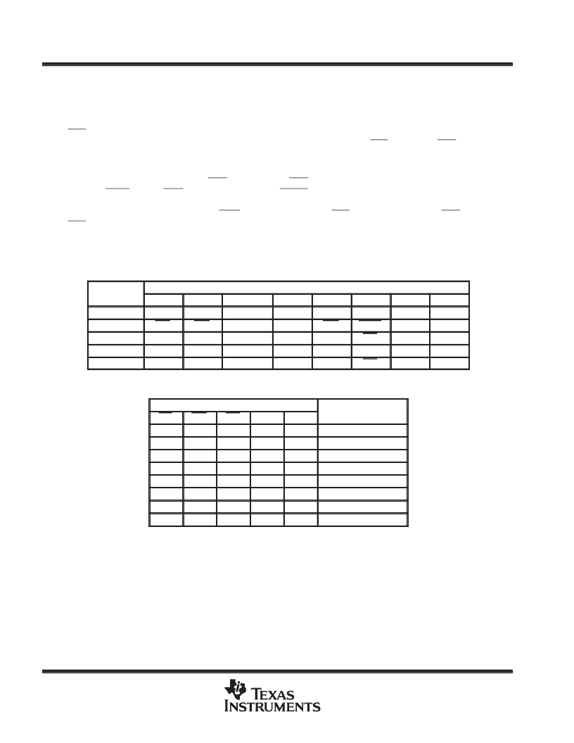
Table 12. Parallel Port Registers
REGISTER
REGISTER BITS
BIT 7
PD7
BIT 6
PD6
BIT 5
PD5
BIT 4
PD4
BIT 3
PD3
BIT 2
PD2
BIT 1
PD1
BIT 0
PD0
Read data
Read status
BSY
ACK
PE
SLCT
ERR
PRINT
1
1
Read control
0
0
PEMD
DIR
PD5
INT2 EN
SLIN
INIT
AFD
STB
Write data
PD7
PD6
PD4
PD3
PD2
PD1
PD0
Write control
0
0
DIR
INT2 EN
SLIN
INIT
AFD
STB
Table 13. Parallel Port Register Select
CONTROL PINS
IOW
CS2
REGISTER SELECTED
IOR
A1
A0
L
H
L
L
L
Read data
L
H
L
L
H
Read status
L
H
L
H
L
Read control
L
H
L
H
H
Invalid
H
L
L
L
L
Write data
H
L
L
L
H
Invalid
H
L
L
H
L
Write control
H
L
L
H
H
Invalid
programmable baud rate generator
The ACE serial channel contains a programmable baud rate generator (BRG) that divides the clock (dc to
8 MHz) by any divisor from 1 to (2
16
–1). The output frequency of the baud generator is 16x the data rate [divisor
# = clock
÷
(baud rate x 16)], referred to in this document as RCLK. Two 8-bit divisor latch registers store the
divisor in a 16-bit binary format. These divisor latch registers must be loaded during initialization. Upon loading
either of the divisor latches, a 16-bit baud counter is immediately loaded. This prevents long counts on initial
load. The BRG can use any of three different popular frequencies to provide standard baud rates. These
frequencies are 1.8432 MHz, 3.072 MHz, and 8 MHz. With these frequencies, standard bit rates from 50 to
512 kbps are available. Tables 14, 15, 16, and 17 illustrate the divisors needed to obtain standard rates using
these three frequencies.
相關(guān)PDF資料 |
PDF描述 |
|---|---|
| TL16C554AI | ASYNCHRONOUS-COMMUNICATIONS ELEMENT |
| TL16C554I | ASYNCHRONOUS COMMUNICATIONS ELEMENT |
| TL2575-15I | 1-A SIMPLE STEP-DOWN SWITCHING VOLTAGE REGULATORS |
| TL2575-33I | 1-A SIMPLE STEP-DOWN SWITCHING VOLTAGE REGULATORS |
| TL2575_0701 | 1-A SIMPLE STEP-DOWN SWITCHING VOLTAGE REGULATORS |
相關(guān)代理商/技術(shù)參數(shù) |
參數(shù)描述 |
|---|---|
| TL16C552AMHV | 制造商:Texas Instruments 功能描述:UART 2-CH 16Byte FIFO 5V 68-Pin CFPAK Tube 制造商:Rochester Electronics LLC 功能描述:DUAL 550 UART WITH CENTRONIX PORT - Bulk |
| TL16C552AMHVB | 制造商:Texas Instruments 功能描述:5962-9755001QXA DUAL 550 UART 制造商:Texas Instruments 功能描述:UART 2-CH 16Byte FIFO 5V 68-Pin CFPAK Tube |
| TL16C552AMPN | 制造商:TI 制造商全稱:Texas Instruments 功能描述:DUAL ASYNCHRONOUS COMMUNICATIONS ELEMENT WITH FIFO |
| TL16C552APN | 功能描述:UART 接口集成電路 Dual UART w/16-Byte FIFOs & Para Port RoHS:否 制造商:Texas Instruments 通道數(shù)量:2 數(shù)據(jù)速率:3 Mbps 電源電壓-最大:3.6 V 電源電壓-最小:2.7 V 電源電流:20 mA 最大工作溫度:+ 85 C 最小工作溫度:- 40 C 封裝 / 箱體:LQFP-48 封裝:Reel |
| TL16C552APNG4 | 功能描述:UART 接口集成電路 Dual UART w/ 16-Byte FIFO RoHS:否 制造商:Texas Instruments 通道數(shù)量:2 數(shù)據(jù)速率:3 Mbps 電源電壓-最大:3.6 V 電源電壓-最小:2.7 V 電源電流:20 mA 最大工作溫度:+ 85 C 最小工作溫度:- 40 C 封裝 / 箱體:LQFP-48 封裝:Reel |
發(fā)布緊急采購,3分鐘左右您將得到回復(fù)。