- 您現(xiàn)在的位置:買賣IC網(wǎng) > PDF目錄384000 > TISPPBL3DR (BOURNS INC) DUAL FORWARD-CONDUCTING P-GATE THYRISTORS FOR ERICSSON MICROELECTRONICS SUBSCRIBER LINE INTERFACE CIRCUITS (SLIC) PDF資料下載
參數(shù)資料
| 型號(hào): | TISPPBL3DR |
| 廠商: | BOURNS INC |
| 元件分類: | 保護(hù)電路 |
| 英文描述: | DUAL FORWARD-CONDUCTING P-GATE THYRISTORS FOR ERICSSON MICROELECTRONICS SUBSCRIBER LINE INTERFACE CIRCUITS (SLIC) |
| 中文描述: | TELECOM, SURGE PROTECTION CIRCUIT, PDSO8 |
| 封裝: | PLASTIC, MS-012, SO-8 |
| 文件頁數(shù): | 6/14頁 |
| 文件大小: | 356K |
| 代理商: | TISPPBL3DR |
OCTOBER 2000 - REVISED FEBRUARY 2005
Specifications are subject to change without notice.
Customers should verify actual device performance in their specific applications.
TISPPBL3 Programmable Protector
Operation of Gated Protectors
The following SLIC circuit definitions are used in this data sheet:
VBAT — Package pin label for the battery supply voltage.
VBat — Voltage applied to the VBAT pin.
VB — Negative power supply voltage applied to the VBAT pin via an isolation diode. This voltage is also the gate reference voltage, VGG, of
the TISPPBL3. When the isolation diode, D1, is conducting, then VBat =VB + 0.7.
The isolation diode, D1 in Figure 5, is to prevent a damaging current flowing into the SLIC substrate (VBAT pin) if the VBat voltage becomes
more negative than the VB supply during a negative overvoltage condition. Each SLIC must have its own isolation diode from the VB voltage
supply. (Maytum, M J, Enoksson, J & Rutgers, K, Coordination of overvoltage protection and SLIC capability, International IC - China
Conference Proceedings 2000, pp. 87 - 97.)
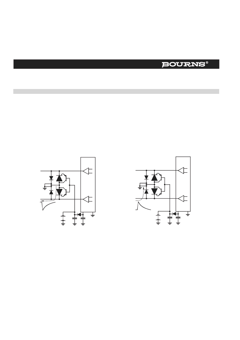
Figure 5 and Figure 6 show how the TISPPBL3 limits overvoltages. The TISPPBL3 thyristor sections limit negative overvoltages and the diode
sections limit positive overvoltages.
Figure 5. Negative Overvoltage Condition
AI6XANB
SLIC
SLIC
PROTECTION
TISPPBLx
C1
V
B
C2
D1
V
Bat
Th4
Th5
I
T
Figure 6. Positive Overvoltage Condition
I
F
AI6XAOB
SLIC
SLIC
PROTECTION
TISPPBLx
C1
V
B
C2
D1
V
Bat
Th4
Th5
Negative overvoltages (Figure 5) are initially clipped close to the SLIC negative supply rail value (VB) by the conduction of the transistor base-
emitter and the thyristor gate-cathode junctions. If sufficient current is available from the overvoltage, then the thyristor will crowbar into a low
voltage ground referenced on-state condition. As the overvoltage subsides, the high holding current of the crowbar thyristor prevents d.c. latchup.
The negative protection voltage will be the sum of the gate supply (VB) and the peak gate (terminal)-cathode voltage (VGK(BO)). Under a.c.
overvoltage conditions VGK(BO) will be less than 3 V. The integrated transistor buffer in the TISPPBL3 greatly reduces the gate positive current
(from about 50 mA to 1 mA) and introduces a negative gate current. Figure 1 shows that the TISPPBL3 gate current depends on the current
being conducted by the principal terminals. The gate current is positive during clipping (charging the VB supply) and negative when the
thyristor is on or the diode is conducting (loading the VB supply). Without the negative gate current and the reduced level of positive gate
current, the VB supply could be charged with a current of nearly 100 mA. The VB supply is likely to be electronic and would not be designed to
be charged like a battery. As a result, the SLIC could be destroyed by the voltage of VB increasing to a level that exceeded the SLIC’s
capability on the VBAT pin. The integrated transistor buffer removes this problem.
Fast rising impulses will cause short term overshoots in gate-cathode voltage. The negative protection voltage under impulse conditions will
also be increased if there is a long connection between the gate decoupling capacitor, C1, and the gate terminal. During the initial rise of a fast
impulse, the gate current (IG) is the same as the cathode current (IK). Rates of 60 A/
μ
s can cause inductive voltages of 0.6 V in 2.5 cm of
printed wiring track. To minimize this inductive voltage increase of protection voltage, the length of the capacitor to gate terminal tracking
should be minimized. Inductive voltages in the protector cathode wiring can increase the protection voltage. These voltages can be minimized
by routing the SLIC connection through the protector as shown in Figure 5 and Figure 6.
Positive overvoltages (Figure 6) are clipped to ground by forward conduction of the diode section in the TISPPBL3. Fast rising impulses will
cause short term overshoots in forward voltage (VFRM).
APPLICATIONS INFORMATION
相關(guān)PDF資料 |
PDF描述 |
|---|---|
| TISPPBL3DR-S | DUAL FORWARD-CONDUCTING P-GATE THYRISTORS FOR ERICSSON MICROELECTRONICS SUBSCRIBER LINE INTERFACE CIRCUITS (SLIC) |
| TISPPBL3D-S | DUAL FORWARD-CONDUCTING P-GATE THYRISTORS FOR ERICSSON MICROELECTRONICS SUBSCRIBER LINE INTERFACE CIRCUITS (SLIC) |
| TITAN19244 | Semiconductor Solutions for High Speed Communications and Fiber Optic Applications |
| TL054AIN | ENHANCED-JFET LOW-OFFSET OPERATIONAL AMPLIFIERS |
| TL05 | ENHANCED-JFET LOW-OFFSET OPERATIONAL AMPLIFIERS |
相關(guān)代理商/技術(shù)參數(shù) |
參數(shù)描述 |
|---|---|
| TISPPBL3DR-S | 功能描述:SCR SURGE SUP 8-SOP RoHS:否 制造商:STMicroelectronics 最大轉(zhuǎn)折電流 IBO:480 A 額定重復(fù)關(guān)閉狀態(tài)電壓 VDRM:600 V 關(guān)閉狀態(tài)漏泄電流(在 VDRM IDRM 下):5 uA 開啟狀態(tài) RMS 電流 (It RMS): 正向電壓下降:1.6 V 柵觸發(fā)電壓 (Vgt):1.3 V 最大柵極峰值反向電壓:5 V 柵觸發(fā)電流 (Igt):35 mA 保持電流(Ih 最大值):75 mA 安裝風(fēng)格:Through Hole 封裝 / 箱體:TO-220 封裝:Tube |
| TISPPBL3D-S | 功能描述:SCR SURGE SUP 8-SOP RoHS:否 制造商:STMicroelectronics 最大轉(zhuǎn)折電流 IBO:480 A 額定重復(fù)關(guān)閉狀態(tài)電壓 VDRM:600 V 關(guān)閉狀態(tài)漏泄電流(在 VDRM IDRM 下):5 uA 開啟狀態(tài) RMS 電流 (It RMS): 正向電壓下降:1.6 V 柵觸發(fā)電壓 (Vgt):1.3 V 最大柵極峰值反向電壓:5 V 柵觸發(fā)電流 (Igt):35 mA 保持電流(Ih 最大值):75 mA 安裝風(fēng)格:Through Hole 封裝 / 箱體:TO-220 封裝:Tube |
| TISPPBL3-S | 功能描述:SCR RoHS:否 制造商:STMicroelectronics 最大轉(zhuǎn)折電流 IBO:480 A 額定重復(fù)關(guān)閉狀態(tài)電壓 VDRM:600 V 關(guān)閉狀態(tài)漏泄電流(在 VDRM IDRM 下):5 uA 開啟狀態(tài) RMS 電流 (It RMS): 正向電壓下降:1.6 V 柵觸發(fā)電壓 (Vgt):1.3 V 最大柵極峰值反向電壓:5 V 柵觸發(fā)電流 (Igt):35 mA 保持電流(Ih 最大值):75 mA 安裝風(fēng)格:Through Hole 封裝 / 箱體:TO-220 封裝:Tube |
| TISPPBL3SE | 功能描述:SCR RoHS:否 制造商:STMicroelectronics 最大轉(zhuǎn)折電流 IBO:480 A 額定重復(fù)關(guān)閉狀態(tài)電壓 VDRM:600 V 關(guān)閉狀態(tài)漏泄電流(在 VDRM IDRM 下):5 uA 開啟狀態(tài) RMS 電流 (It RMS): 正向電壓下降:1.6 V 柵觸發(fā)電壓 (Vgt):1.3 V 最大柵極峰值反向電壓:5 V 柵觸發(fā)電流 (Igt):35 mA 保持電流(Ih 最大值):75 mA 安裝風(fēng)格:Through Hole 封裝 / 箱體:TO-220 封裝:Tube |
| TISPPBL3SE-S | 功能描述:SCR RoHS:否 制造商:STMicroelectronics 最大轉(zhuǎn)折電流 IBO:480 A 額定重復(fù)關(guān)閉狀態(tài)電壓 VDRM:600 V 關(guān)閉狀態(tài)漏泄電流(在 VDRM IDRM 下):5 uA 開啟狀態(tài) RMS 電流 (It RMS): 正向電壓下降:1.6 V 柵觸發(fā)電壓 (Vgt):1.3 V 最大柵極峰值反向電壓:5 V 柵觸發(fā)電流 (Igt):35 mA 保持電流(Ih 最大值):75 mA 安裝風(fēng)格:Through Hole 封裝 / 箱體:TO-220 封裝:Tube |
發(fā)布緊急采購,3分鐘左右您將得到回復(fù)。