- 您現(xiàn)在的位置:買賣IC網(wǎng) > PDF目錄383878 > TAS5036A (Texas Instruments, Inc.) Six Channel Digital Audio PWM Processor PDF資料下載
參數(shù)資料
| 型號: | TAS5036A |
| 廠商: | Texas Instruments, Inc. |
| 英文描述: | Six Channel Digital Audio PWM Processor |
| 中文描述: | 六通道數(shù)字音頻PWM處理器 |
| 文件頁數(shù): | 28/62頁 |
| 文件大?。?/td> | 790K |
| 代理商: | TAS5036A |
第1頁第2頁第3頁第4頁第5頁第6頁第7頁第8頁第9頁第10頁第11頁第12頁第13頁第14頁第15頁第16頁第17頁第18頁第19頁第20頁第21頁第22頁第23頁第24頁第25頁第26頁第27頁當(dāng)前第28頁第29頁第30頁第31頁第32頁第33頁第34頁第35頁第36頁第37頁第38頁第39頁第40頁第41頁第42頁第43頁第44頁第45頁第46頁第47頁第48頁第49頁第50頁第51頁第52頁第53頁第54頁第55頁第56頁第57頁第58頁第59頁第60頁第61頁第62頁
Architecture Overview
22
SLES061B—November 2002—Revised January 2004
TAS5036A
2.4.4 PWM DC-Offset Correction
An 8-bit value can be programmed to each of the six PWM offset correction registers to correct for any offset
present in the output stages. The offset correction is divided into 256 intervals with a total offset correction of
±
1.56% of full scale. The default value is zero correction represented by 00h. These values can be changed
at any time through the serial control interface.
2.4.5 Interchannel Delay
An 8-bit value can be programmed to each of the six PWM interchannel delay registers to add a delay per
channel from 0 to 255 clock cycles. The delays correspond to cycles of the high-speed internal clock, DCLK.
Each subsequent channel has a default value that is N DCLKs larger than the preceding channel. The default
values are 0 for the first channel and 76 for each successive channel.
These values can be updated upon power up through the serial control interface. This delay is generated in
the PWM block with the appropriate control signals generated in the CTL block.
These values can be changed at any time through the serial control interface.
2.4.6 ABD Delay
A 5-bit value is used to delay the A PWM signals with respect to B PWM signals. The value is the same for
all channels. It can be programmed from 0 to 31 DCLK clock cycles. The default value is 17 DCLK clock cycles
(01011). These values can be changed at any time through the serial control interface.
NOTE:
The performance of a PurePath Digital
amplifier system is optimized by setting the PWM
timing based upon the type of back-end device that is used and the layout. These values are
set during initialization using the I
2
C serial interface.
2.4.7 PWM/H-Bridge and Discrete H-Bridge Driver Interface
The TAS5036A provides six PWM outputs, which are designed to drive switching output stages (back-ends)
in both single-ended (SE) and H-bridge (bridge-tied load) configuration. The back ends can be monolithic
power stages (such as the TAS5110) or six discrete differential power stages using gate drivers (such as the
the TAS55182) and MOSFETs in single-ended or bridged configurations.
The TAS5110 device is optimized for bridge-tied load (BTL) configurations. These devices require a pure
differential PWM signal with a third signal (VALID) to control the MUTE state. In the MUTE state, the TAS5110
OUTA and OUTB are both low.
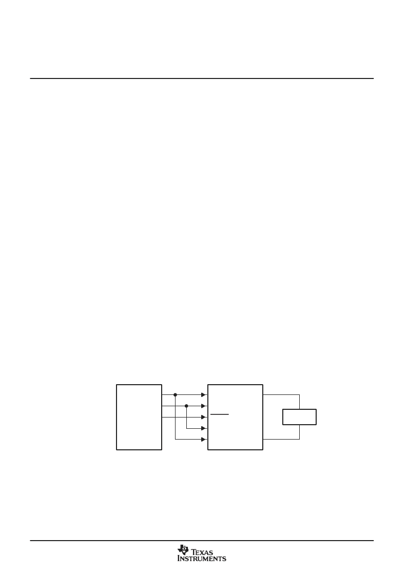
One Channel
of TAS5036A
PWM_AP
PWM_AM
VALID
TAS5110
OUTA
OUTB
AP
AM
RESET
BP
BM
Speaker
Figure 212. PWM Outputs and H-Bridge Driven in BTL Configuration
2.5
I
2
C Serial Control Interface
MCLK must be active for the TAS5036A to support I
2
C bus transactions. The TAS5036A has a bidirectional
serial control interface that is compatible with the I
2
C (Inter IC) bus protocol and supports both 100-kbps and
400-kbps data transfer rates for single- and multiple-byte write and read operations. This is a slave-only device
that does not support a multi-master bus environment or wait state insertion. The control interface is used to
program the registers of the device and to read device status.
PurePath Digital is a trademark of Texas Instruments.
相關(guān)PDF資料 |
PDF描述 |
|---|---|
| TAS5036A_06 | Six Channel Digital Audio PWM Processor |
| TAS5036AIPFC | Six Channel Digital Audio PWM Processor |
| TAS5036AIPFCG4 | Six Channel Digital Audio PWM Processor |
| TAS5036AIPFCR | Six Channel Digital Audio PWM Processor |
| TAS5036AIPFCRG4 | Six Channel Digital Audio PWM Processor |
相關(guān)代理商/技術(shù)參數(shù) |
參數(shù)描述 |
|---|---|
| TAS5036A_06 | 制造商:TI 制造商全稱:Texas Instruments 功能描述:Six Channel Digital Audio PWM Processor |
| TAS5036AIPFC | 功能描述:音頻放大器 Digital Audio PWM Processor RoHS:否 制造商:STMicroelectronics 產(chǎn)品:General Purpose Audio Amplifiers 輸出類型:Digital 輸出功率: THD + 噪聲: 工作電源電壓:3.3 V 電源電流: 最大功率耗散: 最大工作溫度: 安裝風(fēng)格:SMD/SMT 封裝 / 箱體:TQFP-64 封裝:Reel |
| TAS5036AIPFCG4 | 功能描述:音頻放大器 Digital Audio PWM Processor RoHS:否 制造商:STMicroelectronics 產(chǎn)品:General Purpose Audio Amplifiers 輸出類型:Digital 輸出功率: THD + 噪聲: 工作電源電壓:3.3 V 電源電流: 最大功率耗散: 最大工作溫度: 安裝風(fēng)格:SMD/SMT 封裝 / 箱體:TQFP-64 封裝:Reel |
| TAS5036AIPFCR | 功能描述:音頻放大器 Digital Audio PWM Processor RoHS:否 制造商:STMicroelectronics 產(chǎn)品:General Purpose Audio Amplifiers 輸出類型:Digital 輸出功率: THD + 噪聲: 工作電源電壓:3.3 V 電源電流: 最大功率耗散: 最大工作溫度: 安裝風(fēng)格:SMD/SMT 封裝 / 箱體:TQFP-64 封裝:Reel |
| TAS5036AIPFCRG4 | 功能描述:音頻放大器 Digital Audio PWM Processor RoHS:否 制造商:STMicroelectronics 產(chǎn)品:General Purpose Audio Amplifiers 輸出類型:Digital 輸出功率: THD + 噪聲: 工作電源電壓:3.3 V 電源電流: 最大功率耗散: 最大工作溫度: 安裝風(fēng)格:SMD/SMT 封裝 / 箱體:TQFP-64 封裝:Reel |
發(fā)布緊急采購,3分鐘左右您將得到回復(fù)。