- 您現(xiàn)在的位置:買賣IC網(wǎng) > PDF目錄297490 > T630 (Dynex Semiconductor Ltd.) Radiation hard 16-Bit ParallelError Detection & Correction PDF資料下載
參數(shù)資料
| 型號: | T630 |
| 廠商: | Dynex Semiconductor Ltd. |
| 英文描述: | Radiation hard 16-Bit ParallelError Detection & Correction |
| 中文描述: | 輻射硬16位ParallelError檢測 |
| 文件頁數(shù): | 4/10頁 |
| 文件大?。?/td> | 92K |
| 代理商: | T630 |
54HSC/T630
3/10
14
X
13
X
12
X
11
X
10
X
9
X
8
X
16-bit Data Word
Checkword
Bit
CB0
CB1
CB2
CB3
CB4
CB5
2
X
15
X
7
X
6
X
5
X
4
X
1
X
3
X
0
X
The six check bits are partly bits derived from the matrix of data bits as indicated by 'X' for each bit.
Table 3: Check Word Generation
Error Location
DB15
H
L
H
L
CB0
L
H
CB1
H
L
H
CB2
H
L
H
CB3
H
L
H
CB4
H
L
H
CB5
H
L
No
Error
H
DB0
L
H
L
H
DB1
L
H
L
H
DB2
H
L
H
DB3
L
H
L
H
DB4
L
H
L
H
L
H
DB5
H
L
H
L
H
DB6
H
L
H
L
H
DB7
H
L
H
DB8
L
H
L
DB9
L
H
L
H
L
DB10
L
H
L
H
L
DB11
H
L
H
L
H
L
DB12
H
L
H
L
DB13
L
H
L
DB14
H
L
H
L
Syndrome
Error
Code
CB0
CB1
CB2
CB3
CB4
CB5
Table 4: Error Syndrome Codes
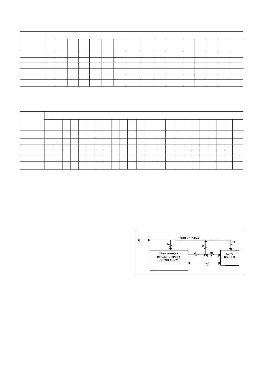
APPLICATIONS
Although many semiconductor memories have separate
input and output pins, it is possible to design the error
detection and correction function using a single EDAC. EDAC
data and check bit pins function as inputs or outputs
dependent upon the state of control signals S0 and S1. It
becomes necessary to use wired AND logic, with fairly
complex timing system, to control the EDAC and data bus.
This scheme becomes difficult to implement both in terms of
board layout and timing. System performance is also
adversely affected, See Figure 2.
Optimised systems can be implemented using two EDAC’s
in parallel, One of the units is used strictly as an encoder
during the memory write cycle. Both controls S0 and Sl are
grounded, The encoder chip will generate the 6-bit check word
for memory storage along with the 16-bit data.
The second of the two EDAC’s will be used as a decoder
during the memory read cycle. This decoder chip requires
timing pulses for correct operation. Control S1 is set low and
S0 high as the memory read cycle begins. After the memory
output data is valid, the control S1 input is moved from the low
to a high. This low-to-high transition latches the 22-bit word
from memory into internal registers of this second EDAC and
enables the two error flags. If no error occurs, the CPU can
accept the 16-bit word directly from memory. If a single error
has occurred, the CPU must move the control SO input from
the high to a low to output corrected data and the error
syndrome bits. Any dual error should be an interrupt condition.
In most applications, status registers will be used to keep
tabs on error flags and error syndrome bits. If repeated
patterns of error flags and syndrome bits occur, the CPU will
be able to recognize these symptoms as a “hard” error. The
syndrome bits can be used to pinpoint the faulty memory chip,
See Figure 3.
Figure 2: Error Detection and Correction Using a
Single EDAC Unit
相關(guān)PDF資料 |
PDF描述 |
|---|---|
| T6A6CI | Bi-Directional Triode Thyristor 6A Mold TRIAC |
| T70HFL10S10 | 70 A, 100 V, SILICON, RECTIFIER DIODE |
| T7NS5D1-18 | POWER/SIGNAL RELAY, SPDT, MOMENTARY, 0.02A (COIL), 18VDC (COIL), 360mW (COIL), 10A (CONTACT), 28VDC (CONTACT), THROUGH HOLE-STRAIGHT MOUNT |
| T85HF120 | 85 A, 1200 V, SILICON, RECTIFIER DIODE |
| T8670VBBB142W | ROCKER SWITCH, DPDT, LATCHED, PANEL MOUNT |
相關(guān)代理商/技術(shù)參數(shù) |
參數(shù)描述 |
|---|---|
| T6300115 | 制造商:POWEREX 制造商全稱:Powerex Power Semiconductors 功能描述:Phase Control SCR (150-300 Amperes 100-1600 Volts) |
| T6300120 | 制造商:POWEREX 制造商全稱:Powerex Power Semiconductors 功能描述:Phase Control SCR (150-300 Amperes 100-1600 Volts) |
| T6300130 | 制造商:POWEREX 制造商全稱:Powerex Power Semiconductors 功能描述:Phase Control SCR (150-300 Amperes 100-1600 Volts) |
| T6300215 | 制造商:POWEREX 制造商全稱:Powerex Power Semiconductors 功能描述:Phase Control SCR (150-300 Amperes 100-1600 Volts) |
| T6300220 | 制造商:POWEREX 制造商全稱:Powerex Power Semiconductors 功能描述:Phase Control SCR (150-300 Amperes 100-1600 Volts) |
發(fā)布緊急采購,3分鐘左右您將得到回復(fù)。