- 您現(xiàn)在的位置:買(mǎi)賣(mài)IC網(wǎng) > PDF目錄383868 > SY89429VZCTR (MICREL INC) 5V/3.3V PROGRAMMABLE FREQUENCY SYNTHESIZER 25MHz to 400MHz PDF資料下載
參數(shù)資料
| 型號(hào): | SY89429VZCTR |
| 廠(chǎng)商: | MICREL INC |
| 元件分類(lèi): | XO, clock |
| 英文描述: | 5V/3.3V PROGRAMMABLE FREQUENCY SYNTHESIZER 25MHz to 400MHz |
| 中文描述: | PLL FREQUENCY SYNTHESIZER, 25 MHz, PDSO28 |
| 封裝: | 0.300 INCH, SOIC-28 |
| 文件頁(yè)數(shù): | 5/9頁(yè) |
| 文件大小: | 140K |
| 代理商: | SY89429VZCTR |
5
ClockWorks
SY89429A
Micrel
M,N
S
_CLOCK
S
_DATA
S
_LOAD
P
_LOAD
M[8:0]
N[1:0]
T2
T1
T0
N1
N0
M8
M7
M6
M5
M4
M3
M2
M1
M0
Last
Bit
PROGRAMMING INTERFACE
Programming the device is accomplished by properly
configuring the internal dividers to produce the desired
frequency at the outputs. The output frequency can be
represented by this formula:
FXTAL
Where F
XTAL
is the crystal frequency, M is the loop divider
modulus, and N is the output divider modulus. Note that it is
possible to select values of M such that the PLL is unable to
achieve loop lock. To avoid this, always make sure that M is
selected to be 200
≤
M
≤
400 for a 16MHz input reference.
M[8:0] and N[1:0] are normally specified once at power-on,
through the parallel interface, and then possibly again through
the serial interface. This approach allows the designer to bring
up the application at one frequency and then change or fine-
tune the clock, as the ability to control the serial interface
becomes available. To minimize transients in the frequency
domain, the output should be varied in the smallest step size
possible.
The TEST output provides visibility for one of several
internal nodes (as determined by the T[1:0] bits in the serial
configuration stream). It is not configurable through the parallel
interface. Although it is possible to select the node that
represents FOUT, the TTL output may not be able to toggle
fast enough for some of the higher output frequencies. The T2,
T1, T0 configuration latches are preset to 000 when P_LOAD
is low, so that the FOUT outputs are as jitter-free as possible.
The serial configuration port can be used to select one of the
alternate functions for this pin.
The Test register is loaded with the first three bits, the N
register with the next two and the M register with the final eight
bits of the data stream on the S_
DATA
input. For each register
the most significant bit is loaded first (T2, N1 and M8).
When T[2:0] is set to 100 the SY89429A is placed in PLL
bypass mode. In this mode the S_
CLOCK
input is fed directly
into the M and N dividers. The N divider drives the FOUT
differential pair and the M counter drives the TEST output pin.
In this mode the S_
CLOCK
input could be used for low speed
board level functional test or debug. Bypassing the PLL and
driving FOUT directly gives the user more control on the test
clocks sent through the clock tree (See detailed Block Diagram).
Because the S_
CLOCK
is a TTL level the input frequency is
limited to 250MHz or less. This means the fastest the FOUT
pin can be toggled via the S_
CLOCK
is 125MHz as the
minimum divide ratio of the N counter is 2. Note that the M
counter output on the TEST output will not be a 50% duty cycle
due to the way the divider is implemented.
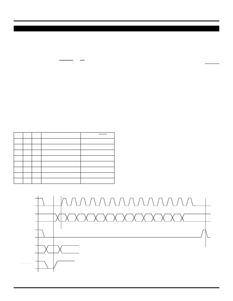
Input S_
DATA
to M0 then M1, then M2, etc., as indicated above.
First
Bit
T2
T1
T0
TEST
FOUT / FOUT
0
0
0
Data Out
–
Last Bit SR
FVCO
÷
N
0
0
1
HIGH
FVCO
÷
N
0
1
0
FREF
FVCO
÷
N
0
1
1
M Counter Output
FVCO
÷
N
1
0
0
FOUT
FVCO
÷
N
1
0
1
LOW
FVCO
÷
N
1
1
0
S_
CLOCK
÷
M
S_
CLOCK
÷
N
1
1
1
FOUT
÷
4
FVCO
÷
N
FOUT = ( ) x
8
M
N
相關(guān)PDF資料 |
PDF描述 |
|---|---|
| SY89429VJC | 5V/3.3V PROGRAMMABLE FREQUENCY SYNTHESIZER 25MHz to 400MHz |
| SY89429VZC | KPSE 10C 10#20 SKT RECP |
| SY89430VJC | 5V/3.3V PROGRAMMABLE FREQUENCY SYNTHESIZER (50MHz to 950MHz) |
| SY89430VJCTR | 5V/3.3V PROGRAMMABLE FREQUENCY SYNTHESIZER (50MHz to 950MHz) |
| SY89430VZC | 5V/3.3V PROGRAMMABLE FREQUENCY SYNTHESIZER (50MHz to 950MHz) |
相關(guān)代理商/技術(shù)參數(shù) |
參數(shù)描述 |
|---|---|
| SY89429VZH | 功能描述:時(shí)鐘合成器/抖動(dòng)清除器 5V/3.3V Programmable Frequency Synthesizer (25-400MHz) (Green) RoHS:否 制造商:Skyworks Solutions, Inc. 輸出端數(shù)量: 輸出電平: 最大輸出頻率: 輸入電平: 最大輸入頻率:6.1 GHz 電源電壓-最大:3.3 V 電源電壓-最小:2.7 V 封裝 / 箱體:TSSOP-28 封裝:Reel |
| SY89429VZH TR | 功能描述:時(shí)鐘合成器/抖動(dòng)清除器 5V/3.3V Programmable Frequency Synthesizer (25-400MHz) (Green) RoHS:否 制造商:Skyworks Solutions, Inc. 輸出端數(shù)量: 輸出電平: 最大輸出頻率: 輸入電平: 最大輸入頻率:6.1 GHz 電源電壓-最大:3.3 V 電源電壓-最小:2.7 V 封裝 / 箱體:TSSOP-28 封裝:Reel |
| SY89429VZHTR | 制造商:MICREL 制造商全稱(chēng):Micrel Semiconductor 功能描述:5V/3.3V PROGRAMMABLE FREQUENCY SYNTHESIZER (25MHz to 400MHz) |
| SY89430 | 制造商:MICREL 制造商全稱(chēng):Micrel Semiconductor 功能描述:5V/3.3V PROGRAMMABLE FREQUENCY SYNTHESIZER (50MHz to 950MHz) |
| SY89430V | 制造商:MICREL 制造商全稱(chēng):Micrel Semiconductor 功能描述:5V/3.3V PROGRAMMABLE FREQUENCY SYNTHESIZER (50MHz to 950MHz) |
發(fā)布緊急采購(gòu),3分鐘左右您將得到回復(fù)。