- 您現在的位置:買賣IC網 > PDF目錄385871 > ST70135 (意法半導體) ASCOTTM DMT TRANSCEIVER PDF資料下載
參數資料
| 型號: | ST70135 |
| 廠商: | 意法半導體 |
| 英文描述: | ASCOTTM DMT TRANSCEIVER |
| 中文描述: | ASCOTTM大唐收發(fā)器 |
| 文件頁數: | 20/29頁 |
| 文件大?。?/td> | 198K |
| 代理商: | ST70135 |
第1頁第2頁第3頁第4頁第5頁第6頁第7頁第8頁第9頁第10頁第11頁第12頁第13頁第14頁第15頁第16頁第17頁第18頁第19頁當前第20頁第21頁第22頁第23頁第24頁第25頁第26頁第27頁第28頁第29頁
ST70135A
20/29
Beware that an incorrect address configuration may lead to bus conflicts. A feature is defined to disable
(tri-state) all outputs of the Utopia interface. It is enabled by the TRI_STATE_EN bit in the Rx_interface
control register.
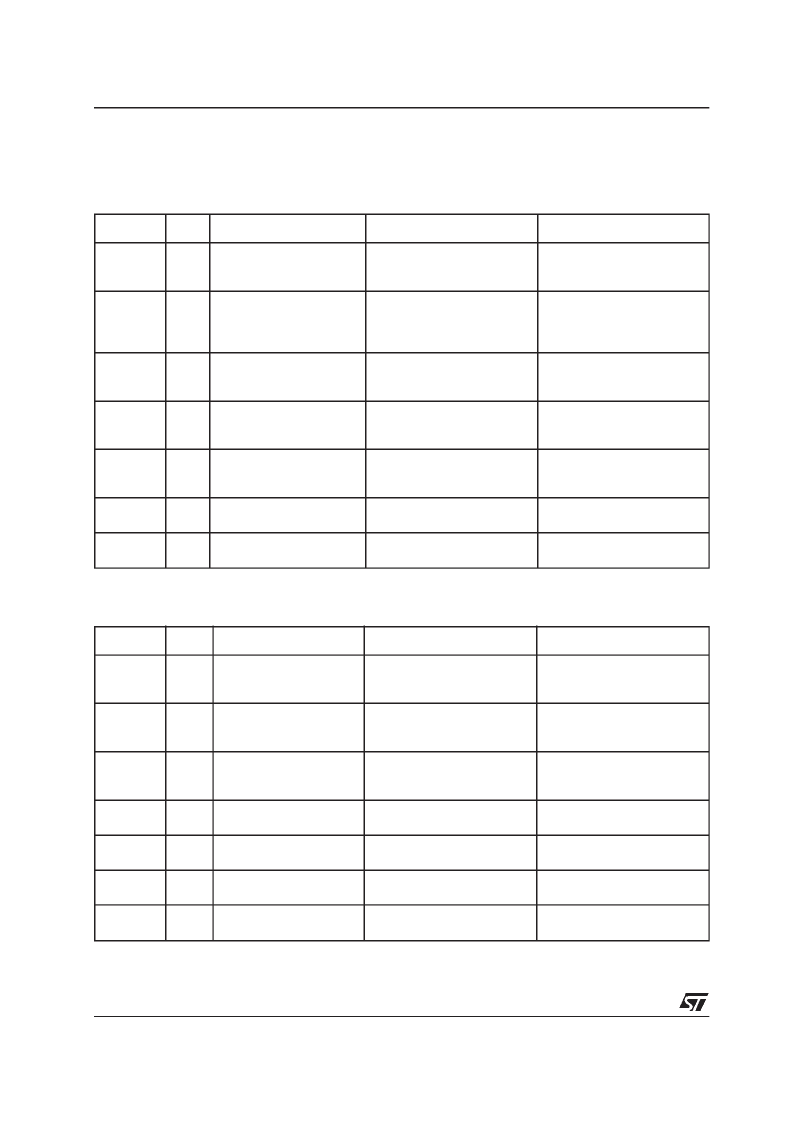
Pin Description Utopia 2 (Receive Interface)
*Active low signal
Pin Description Utopia 2 (Transmit interface)
*Active low signal
Name
Type
Meaning
Usage
Remark
RxClav
O
Receive Cell available
Signals to the ATM chip that
the STLC60135 has a cell
ready for transfer
Remains active for the entire
cell transfer
RxEnb*
I
Receive Enable
Signals to the physical layer
that the ATM chip will sample
and accept data during next
clock cycle
RxData and RxSOC could be
tri-state when RxEnb* is
inactive (high)
RxClk
I
Receive Byte Clock
Gives the timing signal for the
transfer, generated by ATM
layer chip.
RxData
O
Receive Data (8 bits)
ATM cell data, from physical
layer chip to ATM chip, byte
wide.
RxSOC
O
Receive Start Cell
Identifies the cell boundary on
RxData
Indicate to the ATM layer chip
that RxData contains the first
valid byte of a cell.
RxAddr
I
Receive Address (5 bits)
Use to select the port that will
be active or polled
RxRef *
O
Reference Clock
8kHz clock transported over
the network
Name
Type
Meaning
Usage
Remark
TxClav
O
Transmit Cell available
Signals tothe ATM chipthat the
physical layer chip is ready to
accept a cell
Remains active for the entire
cell transfer
TxEnb*
I
Transmit Enable
Signals to the physical layer
that TxData and TxSOCare
valid
TxClk
I
Transmit Byte Clock
Gives the timing signal for the
transfer, generated by ATM
layer chip.
TxData
I
Transmit Data (8 bits)
ATM cell data, to physical layer
chip to ATMchip, byte wide.
TxSOC
I
Transmit Start of Cell
Identifies the cell boundary on
TxData
TxAddr
I
Transmit Address (5 bits)
Use to select the port that will
be active or polled
TxRef *
I
Reference Clock
8kHz clock from the ATM layer
chip
相關PDF資料 |
PDF描述 |
|---|---|
| ST70135A | ASCOTTM DMT TRANSCEIVER |
| ST70136 | CPE ADSL ANALOG FRONT END |
| ST70136B | CPE ADSL ANALOG FRONT END |
| ST70136G | CPE ADSL ANALOG FRONT END |
| ST70137 | UNICORNTM PCI & USB CONTROLLERLESS ADSL DMT TRANSCEIVER |
相關代理商/技術參數 |
參數描述 |
|---|---|
| ST70135A | 制造商:STMicroelectronics 功能描述:Modem Chip Single 144-Pin PQFP |
| ST70136 | 制造商:STMICROELECTRONICS 制造商全稱:STMicroelectronics 功能描述:CPE ADSL ANALOG FRONT END |
| ST70136B | 制造商:STMICROELECTRONICS 制造商全稱:STMicroelectronics 功能描述:CPE ADSL ANALOG FRONT END |
| ST70136G | 制造商:STMICROELECTRONICS 制造商全稱:STMicroelectronics 功能描述:CPE ADSL ANALOG FRONT END |
| ST70136Q | 功能描述:射頻無線雜項 ADSL Analg Front-End RoHS:否 制造商:Texas Instruments 工作頻率:112 kHz to 205 kHz 電源電壓-最大:3.6 V 電源電壓-最小:3 V 電源電流:8 mA 最大功率耗散: 工作溫度范圍:- 40 C to + 110 C 封裝 / 箱體:VQFN-48 封裝:Reel |
發(fā)布緊急采購,3分鐘左右您將得到回復。