- 您現(xiàn)在的位置:買賣IC網(wǎng) > PDF目錄383820 > SN74GTLP1394DR Bus Exchanger PDF資料下載
參數(shù)資料
| 型號: | SN74GTLP1394DR |
| 元件分類: | 通用總線功能 |
| 英文描述: | Bus Exchanger |
| 中文描述: | 總線交換 |
| 文件頁數(shù): | 2/16頁 |
| 文件大?。?/td> | 234K |
| 代理商: | SN74GTLP1394DR |
SN74GTLP1394
2-BIT LVTTL-TO-GTLP ADJUSTABLE-EDGE-RATE BUS TRANSCEIVER
WITH SPLIT LVTTL PORT FEEDBACK PATH, AND SELECTABLE POLARITY
SCES286E
–
OCTOBER 1999
–
REVISED AUGUST 2001
2
POST OFFICE BOX 655303
DALLAS, TEXAS 75265
description (continued)
This device is fully specified for live-insertion applications using I
off
, power-up 3-state, and BIAS V
CC
. The I
off
circuitry disables the outputs, preventing damaging current backflow through the device when it is powered
down. The power-up 3-state circuitry places the outputs in the high-impedance state during power up and power
down, which prevents driver conflict. The BIAS V
CC
circuitry precharges and preconditions the B-port
input/output connections, preventing disturbance of active data on the backplane during card insertion or
removal, and permits true live-insertion capability.
This GTLP device features TI-OPC circuitry, which actively limits the overshoot caused by improperly
terminated backplanes, unevenly distributed cards, or empty slots during low-to-high signal transitions. This
improves signal integrity, which allows adequate noise margin to be maintained at higher frequencies.
High-drive GTLP backplane interface devices feature adjustable edge-rate control (ERC). Changing the ERC
input voltage between GND and V
CC
adjusts the B-port output rise and fall times.
This allows the designer to
optimize system data-transfer rate and signal integrity to the backplane load.
When V
CC
is between 0 and 1.5 V, the device is in the high-impedance state during power up or power down.
However, to ensure the high-impedance state above 1.5 V, the output-enable (OE) input should be tied to V
CC
through a pullup resistor; the minimum value of the resistor is determined by the current-sinking capability of
the driver.
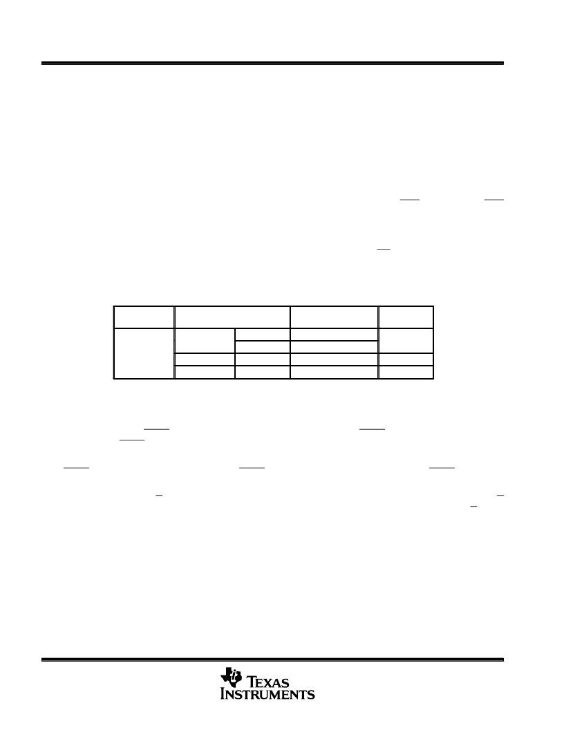
ORDERING INFORMATION
TA
PACKAGE
ORDERABLE
PART NUMBER
TOP-SIDE
MARKING
SOIC
–
D
Tube
SN74GTLP1394D
GTLP1394
–
40
°
C to 85
°
C
Tape and reel
SN74GTLP1394DR
TSSOP
–
PW
Tape and reel
SN74GTLP1394PWR
GP394
TVSOP
–
DGV
Tape and reel
SN74GTLP1394DGVR
GP394
Package drawings, standard packing quantities, thermal data, symbolization, and PCB design
guidelines are available at www.ti.com/sc/package.
functional description
The output-enable (OEAB) input controls the activity of the B port. When OEAB is low, the B-port outputs are
active. When OEAB is high, the B-port outputs are disabled.
Separate LVTTL input and output pins provide a feedback path for control and diagnostics monitoring. The
OEBY input controls the Y outputs. When OEBY is low, the Y outputs are active. When OEBY is high, the
Y outputs are disabled.
The polarity-control (T/C) input is provided to select polarity of data transmission in both directions. When T/C
is high, data transmission is true, and A data goes to the B bus and B data goes to the Y bus. When T/C is low,
data transmission is complementary, and inverted A data goes to the B bus and inverted B data goes to the
Y bus.
相關(guān)PDF資料 |
PDF描述 |
|---|---|
| SN74GTLP1394PWR | Bus Exchanger |
| SN74HC4515DW | 4-To-16-Line Demultiplexer |
| CD74HC10H | Triple 3-input NAND Gate |
| CD74HC112NSR96 | FLIP-FLOP|DUAL|J/K TYPE|HC-CMOS|SOP|16PIN|PLASTIC |
| CD74HC11H | Triple 3-input AND Gate |
相關(guān)代理商/技術(shù)參數(shù) |
參數(shù)描述 |
|---|---|
| SN74GTLP1394DRE4 | 功能描述:轉(zhuǎn)換 - 電壓電平 2-Bit LVTTL/GTLP Bus Xcvr Adj-Edge-Rate RoHS:否 制造商:Micrel 類型:CML/LVDS/LVPECL to LVCMOS/LVTTL 傳播延遲時間:1.9 ns 電源電流:14 mA 電源電壓-最大:3.6 V 電源電壓-最小:3 V 最大工作溫度:+ 85 C 安裝風格:SMD/SMT 封裝 / 箱體:MLF-8 |
| SN74GTLP1394DRG4 | 功能描述:轉(zhuǎn)換 - 電壓電平 2B LVTTL to GTLP Adj Edg RateBus Xcvr RoHS:否 制造商:Micrel 類型:CML/LVDS/LVPECL to LVCMOS/LVTTL 傳播延遲時間:1.9 ns 電源電流:14 mA 電源電壓-最大:3.6 V 電源電壓-最小:3 V 最大工作溫度:+ 85 C 安裝風格:SMD/SMT 封裝 / 箱體:MLF-8 |
| SN74GTLP1394PW | 功能描述:轉(zhuǎn)換 - 電壓電平 2-Bit LVTTL/GTLP Bus Xcvr Adj-Edge-Rate RoHS:否 制造商:Micrel 類型:CML/LVDS/LVPECL to LVCMOS/LVTTL 傳播延遲時間:1.9 ns 電源電流:14 mA 電源電壓-最大:3.6 V 電源電壓-最小:3 V 最大工作溫度:+ 85 C 安裝風格:SMD/SMT 封裝 / 箱體:MLF-8 |
| SN74GTLP1394PWE4 | 功能描述:轉(zhuǎn)換 - 電壓電平 2-Bit LVTTL/GTLP Bus Xcvr Adj-Edge-Rate RoHS:否 制造商:Micrel 類型:CML/LVDS/LVPECL to LVCMOS/LVTTL 傳播延遲時間:1.9 ns 電源電流:14 mA 電源電壓-最大:3.6 V 電源電壓-最小:3 V 最大工作溫度:+ 85 C 安裝風格:SMD/SMT 封裝 / 箱體:MLF-8 |
| SN74GTLP1394PWG4 | 功能描述:轉(zhuǎn)換 - 電壓電平 2B LVTTL to GTLP Adj Edg RateBus Xcvr RoHS:否 制造商:Micrel 類型:CML/LVDS/LVPECL to LVCMOS/LVTTL 傳播延遲時間:1.9 ns 電源電流:14 mA 電源電壓-最大:3.6 V 電源電壓-最小:3 V 最大工作溫度:+ 85 C 安裝風格:SMD/SMT 封裝 / 箱體:MLF-8 |
發(fā)布緊急采購,3分鐘左右您將得到回復。