- 您現(xiàn)在的位置:買賣IC網(wǎng) > PDF目錄373436 > SN54AC374J (Texas Instruments, Inc.) OCTAL D-TYPE EDGE-TRIGGERED FLIP-FLOPS WITH 3-STATE OUTPUTS PDF資料下載
參數(shù)資料
| 型號: | SN54AC374J |
| 廠商: | Texas Instruments, Inc. |
| 英文描述: | OCTAL D-TYPE EDGE-TRIGGERED FLIP-FLOPS WITH 3-STATE OUTPUTS |
| 中文描述: | 八路D型沿觸發(fā)器與觸發(fā)器3態(tài)輸出 |
| 文件頁數(shù): | 2/16頁 |
| 文件大小: | 539K |
| 代理商: | SN54AC374J |
SCAS543E OCTOBER 1995 - REVISED OCTOBER 2003
2
POST OFFICE BOX 655303
DALLAS, TEXAS 75265
description/ordering information (continued)
To ensure the high-impedance state during power up or power down, OE should be tied to V
CC
through a pullup
resistor; the minimum value of the resistor is determined by the current-sinking capability of the driver.
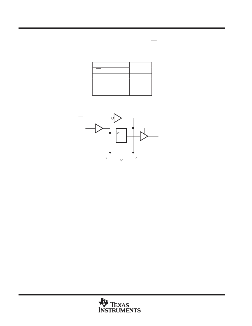
FUNCTION TABLE
(each flip-flop)
INPUTS
OUTPUT
Q
OE
L
CLK
↑
↑
H or L
D
H
H
L
L
L
L
X
Q0
Z
H
X
X
logic diagram (positive logic)
1D
CLK
1Q
2
11
3
1
1D
OE
C1
To Seven Other Channels
absolute maximum ratings over operating free-air temperature range (unless otherwise noted)
Supply voltage range, V
CC
. . . . . . . . . . . . . . . . . . . . . . . . . . . . . . . . . . . . . . . . . . . . . . . . . . . . . . . . . .
Input voltage range, V
I
(see Note 1)
. . . . . . . . . . . . . . . . . . . . . . . . . . . . . . . . . . . . . . . . . . .
Output voltage range, V
O
(see Note 1)
. . . . . . . . . . . . . . . . . . . . . . . . . . . . . . . . . . . . . . . .
Input clamp current, I
IK
(V
I
< 0 or V
I
> V
CC)
. . . . . . . . . . . . . . . . . . . . . . . . . . . . . . . . . . . . . . . . . . . . . . . .
Output clamp current, I
OK
(V
O
< 0 or V
O
> V
CC)
. . . . . . . . . . . . . . . . . . . . . . . . . . . . . . . . . . . . . . . . . . . .
Continuous output current, I
O
(V
O
= 0 to V
CC
)
. . . . . . . . . . . . . . . . . . . . . . . . . . . . . . . . . . . . . . . . . . . . . .
Continuous current through V
CC
or GND
. . . . . . . . . . . . . . . . . . . . . . . . . . . . . . . . . . . . . . . . . . . . . . . . . .
Package thermal impedance,
θ
JA
(see Note 2): DB package
DW package
N package
NS package
PW package
Storage temperature range, T
stg
. . . . . . . . . . . . . . . . . . . . . . . . . . . . . . . . . . . . . . . . . . . . . . . . . . .
0.5 V to 7 V
0.5 V to V
CC
+ 0.5 V
0.5 V to V
CC
+ 0.5 V
±
20 mA
±
20 mA
±
50 mA
±
200 mA
70
°
C/W
58
°
C/W
69
°
C/W
60
°
C/W
83
°
C/W
. . . . . . . . . . . . . . . . . . . . . . . . . . . . . . . . .
. . . . . . . . . . . . . . . . . . . . . . . . . . . . . . . . .
. . . . . . . . . . . . . . . . . . . . . . . . . . . . . . . . . . .
. . . . . . . . . . . . . . . . . . . . . . . . . . . . . . . . .
. . . . . . . . . . . . . . . . . . . . . . . . . . . . . . . . .
65
°
C to 150
°
C
Stresses beyond those listed under “absolute maximum ratings” may cause permanent damage to the device. These are stress ratings only, and
functional operation of the device at these or any other conditions beyond those indicated under “recommended operating conditions” is not
implied. Exposure to absolute-maximum-rated conditions for extended periods may affect device reliability.
NOTES:
1. The input and output voltage ratings may be exceeded if the input and output current ratings are observed.
2. The package thermal impedance is calculated in accordance with JESD 51-7.
相關(guān)PDF資料 |
PDF描述 |
|---|---|
| SN74AC374DB | Low-Voltage CMOS Hex Inverter; Package: TSSOP-14; No of Pins: 14; Container: Tape and Reel; Qty per Container: 2500 |
| SN54AC374W | OCTAL D-TYPE EDGE-TRIGGERED FLIP-FLOPS WITH 3-STATE OUTPUTS |
| SN54AC533FK | OCTAL TRANSPARENT D-TYPE LATCHES WITH 3-STATE OUTPUTS |
| SN74AC533DB | OCTAL TRANSPARENT D-TYPE LATCHES WITH 3-STATE OUTPUTS |
| SN74AC533PWR | Low-Voltage CMOS Hex Buffer with Open Drain Outputs and 5V-Tolerant Inputs; Package: TSSOP-14; No of Pins: 14; Container: Tape and Reel; Qty per Container: 2500 |
相關(guān)代理商/技術(shù)參數(shù) |
參數(shù)描述 |
|---|---|
| SN54AC374W | 制造商:TI 制造商全稱:Texas Instruments 功能描述:OCTAL D-TYPE EDGE-TRIGGERED FLIP-FLOPS WITH 3-STATE OUTPUTS |
| SN54AC533 | 制造商:TI 制造商全稱:Texas Instruments 功能描述:OCTAL TRANSPARENT D-TYPE LATCHES WITH 3-STATE OUTPUTS |
| SN54AC533FK | 制造商:TI 制造商全稱:Texas Instruments 功能描述:OCTAL TRANSPARENT D-TYPE LATCHES WITH 3-STATE OUTPUTS |
| SN54AC533J | 制造商:TI 制造商全稱:Texas Instruments 功能描述:OCTAL TRANSPARENT D-TYPE LATCHES WITH 3-STATE OUTPUTS |
| SN54AC533W | 制造商:TI 制造商全稱:Texas Instruments 功能描述:OCTAL TRANSPARENT D-TYPE LATCHES WITH 3-STATE OUTPUTS |
發(fā)布緊急采購,3分鐘左右您將得到回復(fù)。