- 您現(xiàn)在的位置:買賣IC網(wǎng) > PDF目錄374797 > SK100LVE111E (Semtech Corporation) CRYSTAL 25.0 MHZ 20PF SMD PDF資料下載
參數(shù)資料
| 型號: | SK100LVE111E |
| 廠商: | Semtech Corporation |
| 英文描述: | CRYSTAL 25.0 MHZ 20PF SMD |
| 中文描述: | 低電壓1:9差動ECL / PECL的時鐘使能輸入驅(qū)動器 |
| 文件頁數(shù): | 5/6頁 |
| 文件大?。?/td> | 150K |
| 代理商: | SK100LVE111E |
SE
H
Today's Results
...
Tomorrow's Vision
SK10LVE111E
SK100LVE111E
Low Voltage 1:9 Differential ECL/PECL
Clock Driver with Enable Input
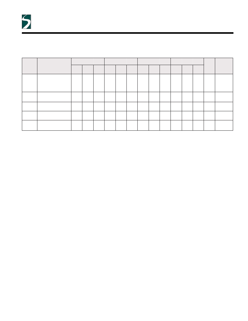
AC Characteristics
(V
EE
= V
EE
(min) to V
EE
(max); V
CC
= V
CCO
= GND)
(Note 4)
- 0
4
o
C
0
o
C
5
2
o
C
5
8
o
C
l
b
m
y
S
c
e
a
r
a
h
C
n
M
p
y
T
x
a
M
n
M
p
y
T
x
a
M
n
M
p
y
T
x
a
M
n
M
p
y
T
x
a
M
t
U
d
n
o
C
t
t
H
L
L
H
P
P
o
y
a
D
n
o
g
t
p
O
(
N
I
n
(
N
I
a
p
o
P
)
n
E
e
D
-
)
e
d
0
0
0
5
4
3
0
0
5
0
6
7
5
5
3
8
4
3
5
5
2
7
6
6
0
0
4
9
4
3
0
0
3
8
6
6
5
5
4
9
4
3
5
5
3
8
6
6
s
p
.
.
t
w
e
k
s
w
D
(
e
k
w
S
e
e
S
c
e
t
P
D
-
W
-
P
)
k
0
5
0
5
2
0
5
0
5
2
0
5
0
5
2
0
5
0
5
2
s
p
.
1
P
P
g
n
w
S
t
p
n
m
u
m
i
M
0
0
5
0
0
5
0
0
5
0
0
5
V
m
.
1
V
R
M
C
e
g
n
a
R
e
d
o
M
n
o
m
m
o
C
- 5
- 4
- 5
- 4
- 5
- 4
- 5
- 4
V
.
1
t
r
t
f
e
%
m
0
8
i
l
%
F
s
R
2
o
0
0
0
2
0
0
6
0
0
2
0
0
6
0
0
2
0
0
6
0
0
2
0
0
6
s
p
%
0
2
-
%
0
8
Notes:
1.
10LVE111E circuits are designed to meet the DC specifications shown in the table after thermal equilibrium has been
established.
The circuit is in a test socket or mounted on a printed circuit board and transverse airflow greater than 500 lfpm is maintained.
Outputs are termionated through a 50
resistor to –2.0V.
The same DC parameter values apply across the full VEE range of –3.0 to –3.8V. Outputs are terminated through a 50
resistor to –2.0V. 100LVE111E circuits are designed to meet the DC specifications shown in the table where transverse airflow
greater than 500 lfpm is maintained.
Absolute maximum rating, beyond which device life may be impaired unless otherwise specificed on an individual data sheet.
Parametric values specified at:
10LVE111E Series: –3.0 to –3.8V
100 LVE111E Series: –3.0 to –3.8V; PECL Power Supply: +3.0V to +3.8V
Guaranteed HIGH signal for all inputs.
Guaranteed LOW signal for all inputs.
These values are for VCC = 3.3V. Level Specifications will vary 1:1 with VCC.
The differential propagation delay is defined as the delay from the crossing points of the differential input signals to the crossing
point of the differential output signals.
The single-ended propagation delay is defined as the delay from the 50% point of the input signal to the 50% point of theoutput
signal.
10. The within-device skew is defined as the worst case difference between any two similar delay paths within a single device.
11. V
PP
(min) is defined as the minimum input differential voltage which will cause no increase in the propagation delay. The
V
PP
(min) is AC limited for the E111 as a differential input as low as 50 mV will still produce full ECL levels at the output.
12. V
CMR
is defined as the range within which the V
IH
level may vary, with the device still meeting the propagation delay
specification. The V
IL
level must be such that the peak-to-peak voltage is less than 1.0V and greater than or equal to
V
PP
(min).
2.
3.
4.
5.
6.
7.
8.
9.
相關(guān)PDF資料 |
PDF描述 |
|---|---|
| SK10LVE111 | CRYSTAL 22.1184 MHZ 20PF SMD |
| SK10LVEL58 | 2:1Multiplexer(10K系列,2:1多路復用器) |
| SK100LVEL58 | 2:1Multiplexer(100K系列,2:1多路復用器) |
| SK1119 | N CHANNEL MOS TYPE (HIGH SPEED, HIGH CURRENT SWITCHING, DC-DC CONVERTER AND MOTOR DRIVE APPLICATIONS) |
| SK14B | 1.0 AMPS. Surface Mount Schottky Barrier Rectifiers |
相關(guān)代理商/技術(shù)參數(shù) |
參數(shù)描述 |
|---|---|
| SK100M0010AZF-0511 | 制造商:Yageo Corporation 功能描述: |
| SK100M0010AZF-0611 | 制造商:Yageo Corporation 功能描述: |
| SK100M0010B2F-0511 | 制造商:Yageo Corporation 功能描述: |
| SK100M0010BZF-0611 | 制造商:Yageo Corporation 功能描述:SK Series 10 uF 100 V 20 % Radial Through Hole Aluminum Electrolytic Capacitor 制造商:Yageo / Phycomp 功能描述:SK radial Al electrolytic cap,10uF 100V 制造商:Yageo 功能描述:Cap Aluminum 10uF 100V 20% (6.3 X 11mm) Radial Aluminum Cylindrical Can 2.5mm 75mA 2000 hr 85 制造商:Yageo 功能描述:Cap Aluminum 10uF 100V 20% (6.3 X 11mm) Radial 2.5mm 75mA 2000h 85°C Bulk |
| SK100M0022A5F-0611 | 制造商:Yageo Corporation 功能描述: |
發(fā)布緊急采購,3分鐘左右您將得到回復。