- 您現(xiàn)在的位置:買賣IC網(wǎng) > PDF目錄2016 > SI5010-B-GM (Silicon Laboratories Inc)IC CLOCK/DATA RECOVERY LP 20-QFN PDF資料下載
參數(shù)資料
| 型號(hào): | SI5010-B-GM |
| 廠商: | Silicon Laboratories Inc |
| 文件頁數(shù): | 10/20頁 |
| 文件大?。?/td> | 0K |
| 描述: | IC CLOCK/DATA RECOVERY LP 20-QFN |
| 標(biāo)準(zhǔn)包裝: | 75 |
| 系列: | DSPLL® |
| 類型: | 時(shí)鐘和數(shù)據(jù)恢復(fù)(CDR) |
| PLL: | 是 |
| 主要目的: | SONET/SDH,ATM 應(yīng)用 |
| 輸入: | 時(shí)鐘 |
| 輸出: | CML |
| 電路數(shù): | 1 |
| 比率 - 輸入:輸出: | 1:2 |
| 差分 - 輸入:輸出: | 是/是 |
| 頻率 - 最大: | 666MHz |
| 電源電壓: | 2.375 V ~ 2.625 V |
| 工作溫度: | -40°C ~ 85°C |
| 安裝類型: | 表面貼裝 |
| 封裝/外殼: | 20-VFQFN 裸露焊盤 |
| 供應(yīng)商設(shè)備封裝: | 20-QFN(4x4) |
| 包裝: | 管件 |
| 產(chǎn)品目錄頁面: | 628 (CN2011-ZH PDF) |
| 其它名稱: | 336-1743-5 |
Si5010
18
Rev. 1.4
9.
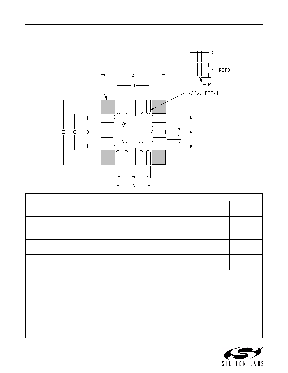
4x4 mm 20L QFN Recommended PCB Layout
Symbol
Parameter
Dimensions
Min
Nom
Max
A
Pad Row/Column Width/Length
2.23
2.25
2.28
D
Thermal Pad Width/Height
2.03
2.08
2.13
e
Pad Pitch
—
0.50 BSC
—
G
Pad Row/Column Separation
2.43
2.46
2.48
R
Pad Radius
—
0.12 REF
—
X
Pad Width
0.23
0.25
0.28
Y
Pad Length
—
0.94 REF
—
Z
Pad Row/Column Extents
4.26
4.28
4.31
Notes:
1.
All dimensions listed are in millimeters (mm).
2.
The perimeter pads are to be Non-Solder Mask Defined (NSMD). Solder mask openings should be designed to leave 60-75 mm
separation between solder mask and pad metal, all the way around the pad.
3.
The center thermal pad is to be Solder Mask Defined (SMD).
4.
Thermal/Ground vias placed in the center pad should be no less than 0.2 mm (8 mil) diameter and tented from the top to prevent
solder from flowing into the via hole.
5.
The stencil aperture should match the pad size (1:1 ratio) for the perimeter pads. A 3x3 array of 0.5 mm square stencil openings, on a
0.65 mm pitch, should be used for the center thermal pad.
6.
A stencil thickness of 5 mil is recommended. The stencil should be laser cut and electropolished, with trapezoidal walls to facilitate
paste release.
7.
A “No-Clean”, Type 3 solder paste should be used for assembly. Nitrogen purge during reflow is recommended.
8.
Do not place any signal or power plane vias in these “keep out” regions.
9.
Suggest four 0.38 mm (15 mil) vias to the ground plane.
See Note 8
Gnd
P
in
Gnd Pin
Gnd
P
in
See Note 9
相關(guān)PDF資料 |
PDF描述 |
|---|---|
| SI5013-D-GM | IC CLOCK/DATA RECOVERY 28MLP |
| SI5017-D-GM | IC CLOCK/DATA RECOVERY 28MLP |
| SI5018-B-GM | IC CLOCK/DATA RECOVERY 20-QFN |
| SI5020-B-GM | IC CLK DATA REC SONET/SDH 20-QFN |
| SI5023-D-GM | IC CLOCK/DATA RECVRY W/AMP 28MLP |
相關(guān)代理商/技術(shù)參數(shù) |
參數(shù)描述 |
|---|---|
| SI5010-B-GMR | 功能描述:時(shí)鐘發(fā)生器及支持產(chǎn)品 OC-3/12 STM-1/4 Sonet/SDH CDR RoHS:否 制造商:Silicon Labs 類型:Clock Generators 最大輸入頻率:14.318 MHz 最大輸出頻率:166 MHz 輸出端數(shù)量:16 占空比 - 最大:55 % 工作電源電壓:3.3 V 工作電源電流:1 mA 最大工作溫度:+ 85 C 安裝風(fēng)格:SMD/SMT 封裝 / 箱體:QFN-56 |
| SI5010-BM | 功能描述:計(jì)時(shí)器和支持產(chǎn)品 SONET/SDH 2.5 V OC-3/12 STM-1/4 RoHS:否 制造商:Micrel 類型:Standard 封裝 / 箱體:SOT-23 內(nèi)部定時(shí)器數(shù)量:1 電源電壓-最大:18 V 電源電壓-最小:2.7 V 最大功率耗散: 最大工作溫度:+ 85 C 最小工作溫度:- 40 C 封裝:Reel |
| SI5010-BMR | 功能描述:計(jì)時(shí)器和支持產(chǎn)品 SONET/SDH 2.5 V OC-3/12 STM-1/4 RoHS:否 制造商:Micrel 類型:Standard 封裝 / 箱體:SOT-23 內(nèi)部定時(shí)器數(shù)量:1 電源電壓-最大:18 V 電源電壓-最小:2.7 V 最大功率耗散: 最大工作溫度:+ 85 C 最小工作溫度:- 40 C 封裝:Reel |
| SI5010-EVB | 功能描述:時(shí)鐘和定時(shí)器開發(fā)工具 SONET/SDH 2.5 V OC-3/12 STM-1/4 RoHS:否 制造商:Texas Instruments 產(chǎn)品:Evaluation Modules 類型:Clock Conditioners 工具用于評(píng)估:LMK04100B 頻率:122.8 MHz 工作電源電壓:3.3 V |
| SI5010-GM | 制造商:SILABS 制造商全稱:SILABS 功能描述:OC-12/3, STM-4/1 SONET/SDH CLOCK AND DATA RECOVERY IC |
發(fā)布緊急采購,3分鐘左右您將得到回復(fù)。