- 您現(xiàn)在的位置:買賣IC網(wǎng) > PDF目錄374734 > SC617 (Semtech Corporation) Charge Pump Flash LED Driver with Safety Timer PDF資料下載
參數(shù)資料
| 型號(hào): | SC617 |
| 廠商: | Semtech Corporation |
| 英文描述: | Charge Pump Flash LED Driver with Safety Timer |
| 中文描述: | 充電泵閃光LED驅(qū)動(dòng)器的安全定時(shí)器 |
| 文件頁(yè)數(shù): | 3/13頁(yè) |
| 文件大小: | 219K |
| 代理商: | SC617 |
第1頁(yè)第2頁(yè)當(dāng)前第3頁(yè)第4頁(yè)第5頁(yè)第6頁(yè)第7頁(yè)第8頁(yè)第9頁(yè)第10頁(yè)第11頁(yè)第12頁(yè)第13頁(yè)
SC617
3
Exceeding the above specifications may result in permanent damage to the device or device malfunction. Operation outside of the parameters
specified in the Electrical Characteristics section is not recommended.
NOTES:
(1) Tested according to JEDEC standard JESD22-A114-B.
(2) Calculated from package in still air, mounted to 3 x 4.5 (in), 4 layer FR4 PCB with thermal vias under the exposed pad per JESD51 standards.
Absolute Maximum Ratings
VIN (V) . . . . . . . . . . . . . . . . . . . . . . . . . . . . . . . . . . . . -0.3 to +6.5
VOUT (V) . . . . . . . . . . . . . . . . . . . . . . . . . . . . . . . . . . -0.3 to +6.5
C1+, C2+ (V) . . . . . . . . . . . . . . . . . . . . . . . -0.3 to (V
OUT
+ 0.3)
Pin Voltage - All Other Pins (V) . . . . . . -0.3 to (V
IN
+ 0.3)
Circuit Duration . . . . . . . . . . . . . . . . . . . . . . . . . . . . Continuous
ESD Protection Level
(1)
(kV) . . . . . . . . . . . . . . . . . . . . . . . . . . . . 2
Recommended Operating Conditions
Ambient Temperature Range (°C) . . . . . . . . . . . -40 to +85
Thermal Information
Thermal Resistance, Junction to Ambient
(2)
(°C/W) . . . .
40
Junction Temperature Range (°C) . . . . . . . . . . . . -40 to +150
Storage Temperature Range (°C) . . . . . . . . . . . . -60 to +150
Peak IR Reflow Temperature (10s to 30s) (°C) . . . . . . +260
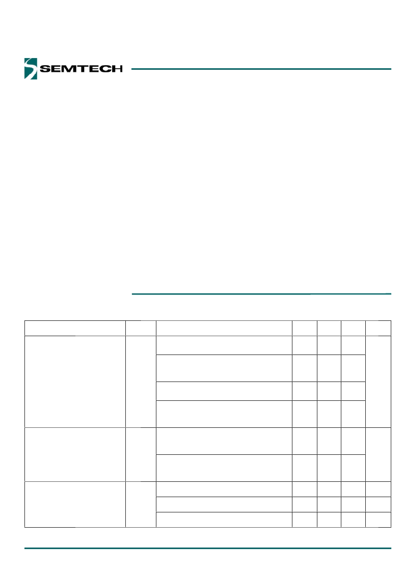
Unless otherwise specified: T
= 25°C for TYP, -40°C to +60°C for MIN and MAX; C
BUCKET
= C
OUT
= 1.0μF (ESR < 0.1Ω); C
IN
= 10.0μF; V
IN
= 3.0V to 5.25V;
V
OUT
= 2.8V to 4.25V; R
SET
= 0.5Ω (0.1%).
Parameter
Symbol
Conditions
Min
Typ
Max
Units
Output Current
I
OUT
FLASH high, R
= 0.357Ω
3.7V < V
IN
< 4.2V, V
OUT
= 3.7V
(1)
FLASH high, R
= 0.5Ω
3.3V < V
IN
< 4.2V
2.8V < V
OUT
< 4.25V
FLASH low, CTRL high, R
= 0.357Ω
3.7V < V
IN
< 4.2V, V
OUT
= 3.4V
(1)
FLASH low, CTRL high, R
SET
= 0.5Ω
3.0V < V
IN
< 4.5V
2.8V < V
OUT
< 4.5V
FLASH high, R
= 0.5Ω
3.3V < V
IN
< 4.2V
2.8V < V
OUT
< 4.25V
FLASH low, CTRL high, R
SET
= 0.5Ω
3.0V < V
IN
< 4.5V
2.8V < V
OUT
< 4.5V
700
mA
460
500
540
210
120
150
180
ISET Reference Voltage
V
ISET
230
250
270
mV
60
75
90
Quiescent Current
I
Q
FLASH high
3.4
5.0
mA
FLASH low, CTRL high
2.0
4.5
mA
FLASH low, CTRL low
0.1
2.0
μA
Electrical Characteristics
相關(guān)PDF資料 |
PDF描述 |
|---|---|
| SC617EVB | Charge Pump Flash LED Driver with Safety Timer |
| SC617ULTRT | Charge Pump Flash LED Driver with Safety Timer |
| SC618 | Charge Pump Flash LED Driver with Safety Timer |
| SC618EVB | Charge Pump Flash LED Driver with Safety Timer |
| SC618ULTRT | Charge Pump Flash LED Driver with Safety Timer |
相關(guān)代理商/技術(shù)參數(shù) |
參數(shù)描述 |
|---|---|
| SC617EVB | 制造商:SEMTECH 制造商全稱:Semtech Corporation 功能描述:Charge Pump Flash LED Driver with Safety Timer |
| SC617ULTRT | 制造商:SEMTECH 制造商全稱:Semtech Corporation 功能描述:Charge Pump Flash LED Driver with Safety Timer |
| SC618 | 制造商:SEMTECH 制造商全稱:Semtech Corporation 功能描述:Charge Pump Flash LED Driver with Safety Timer |
| SC618_08 | 制造商:SEMTECH 制造商全稱:Semtech Corporation 功能描述:Charge Pump Flash LED Driver with Safety Timer |
| SC618EVB | 制造商:SEMTECH 制造商全稱:Semtech Corporation 功能描述:Charge Pump Flash LED Driver with Safety Timer |
發(fā)布緊急采購(gòu),3分鐘左右您將得到回復(fù)。