- 您現(xiàn)在的位置:買賣IC網(wǎng) > PDF目錄374671 > S71PL064J80 (Spansion Inc.) STACKED MULTI CHIP PRODUCT FLASH MEMORY AND RAM PDF資料下載
參數(shù)資料
| 型號(hào): | S71PL064J80 |
| 廠商: | Spansion Inc. |
| 英文描述: | STACKED MULTI CHIP PRODUCT FLASH MEMORY AND RAM |
| 中文描述: | 堆疊式多芯片產(chǎn)品,閃存和RAM |
| 文件頁數(shù): | 76/196頁 |
| 文件大?。?/td> | 5729K |
| 代理商: | S71PL064J80 |
第1頁第2頁第3頁第4頁第5頁第6頁第7頁第8頁第9頁第10頁第11頁第12頁第13頁第14頁第15頁第16頁第17頁第18頁第19頁第20頁第21頁第22頁第23頁第24頁第25頁第26頁第27頁第28頁第29頁第30頁第31頁第32頁第33頁第34頁第35頁第36頁第37頁第38頁第39頁第40頁第41頁第42頁第43頁第44頁第45頁第46頁第47頁第48頁第49頁第50頁第51頁第52頁第53頁第54頁第55頁第56頁第57頁第58頁第59頁第60頁第61頁第62頁第63頁第64頁第65頁第66頁第67頁第68頁第69頁第70頁第71頁第72頁第73頁第74頁第75頁當(dāng)前第76頁第77頁第78頁第79頁第80頁第81頁第82頁第83頁第84頁第85頁第86頁第87頁第88頁第89頁第90頁第91頁第92頁第93頁第94頁第95頁第96頁第97頁第98頁第99頁第100頁第101頁第102頁第103頁第104頁第105頁第106頁第107頁第108頁第109頁第110頁第111頁第112頁第113頁第114頁第115頁第116頁第117頁第118頁第119頁第120頁第121頁第122頁第123頁第124頁第125頁第126頁第127頁第128頁第129頁第130頁第131頁第132頁第133頁第134頁第135頁第136頁第137頁第138頁第139頁第140頁第141頁第142頁第143頁第144頁第145頁第146頁第147頁第148頁第149頁第150頁第151頁第152頁第153頁第154頁第155頁第156頁第157頁第158頁第159頁第160頁第161頁第162頁第163頁第164頁第165頁第166頁第167頁第168頁第169頁第170頁第171頁第172頁第173頁第174頁第175頁第176頁第177頁第178頁第179頁第180頁第181頁第182頁第183頁第184頁第185頁第186頁第187頁第188頁第189頁第190頁第191頁第192頁第193頁第194頁第195頁第196頁
76
S29PL127J/S29PL064J/S29PL032J for MCP
S29PL127J_064J_032J_MCP_00_A3 August 12, 2004
A d v a n c e I n f o r m a t i o n
RY/BY#: Ready/Busy#
The RY/BY# is a dedicated, open-drain output pin which indicates whether an
Embedded Algorithm is in progress or complete. The RY/BY# status is valid after
the rising edge of the final WE# pulse in the command sequence. Since RY/BY#
is an open-drain output, several RY/BY# pins can be tied together in parallel with
a pull-up resistor to V
CC
.
If the output is low (Busy), the device is actively erasing or programming. (This
includes programming in the Erase Suspend mode.) If the output is high (Ready),
the device is in the read mode, the standby mode, or one of the banks is in the
erase-suspend-read mode.
Table
19
shows the outputs for RY/BY#.
DQ6: Toggle Bit I
Toggle Bit I on DQ6 indicates whether an Embedded Program or Erase algorithm
is in progress or complete, or whether the device has entered the Erase Suspend
mode. Toggle Bit I may be read at any address, and is valid after the rising edge
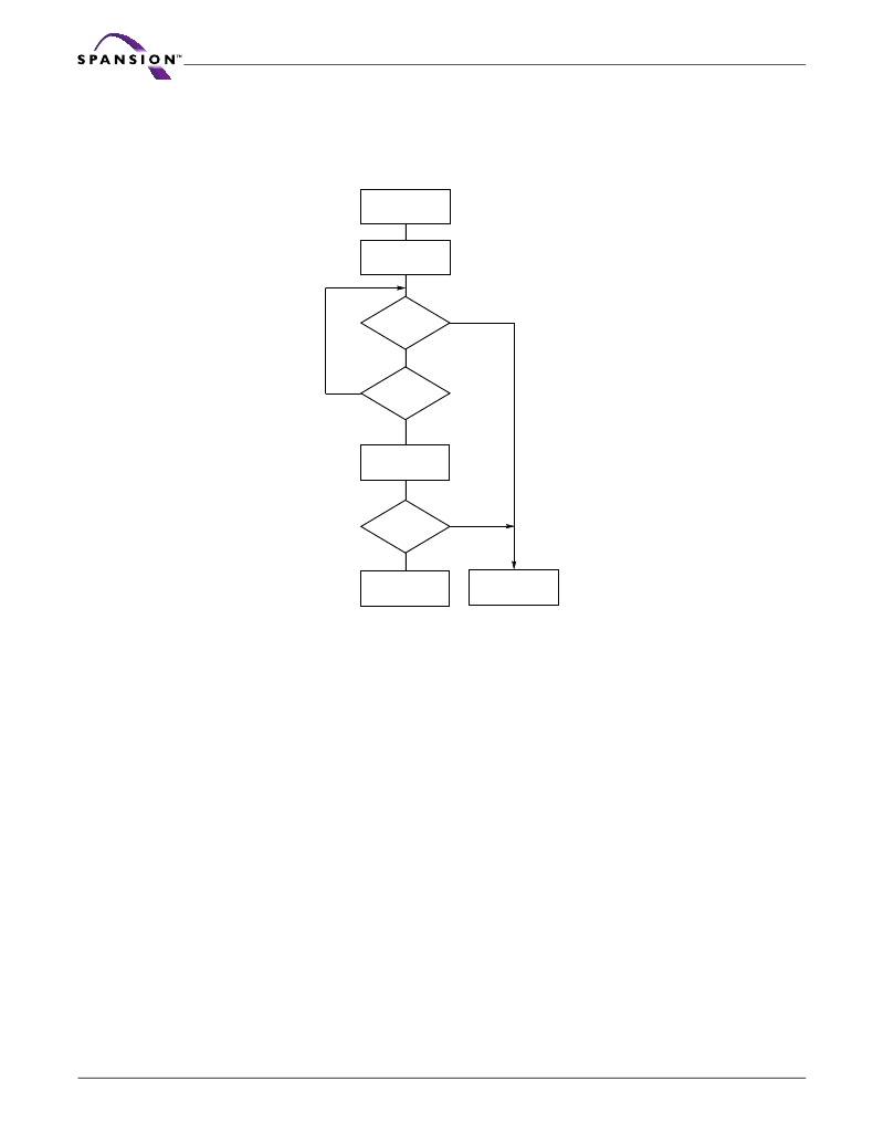
Notes:
1. VA = Valid address for programming. During a sector erase operation, a valid address is
any sector address within the sector being erased. During chip erase, a valid address is
any non-protected sector address.
2. DQ7 should be rechecked even if DQ5 = “1” because DQ7 may change simultaneously
with DQ5.
Figure 6. Data# Polling Algorithm
DQ7 = Data
Yes
No
No
DQ5 = 1
No
Yes
Yes
FAIL
PASS
Read DQ7–DQ0
Addr = VA
Read DQ7–DQ0
Addr = VA
DQ7 = Data
START
相關(guān)PDF資料 |
PDF描述 |
|---|---|
| S71PL064J80-07 | STACKED MULTI CHIP PRODUCT FLASH MEMORY AND RAM |
| S71PL064J80-0K | STACKED MULTI CHIP PRODUCT FLASH MEMORY AND RAM |
| S71PL064J80-0P | STACKED MULTI CHIP PRODUCT FLASH MEMORY AND RAM |
| S71PL064JA0 | STACKED MULTI CHIP PRODUCT FLASH MEMORY AND RAM |
| S71PL064JA0-07 | STACKED MULTI CHIP PRODUCT FLASH MEMORY AND RAM |
相關(guān)代理商/技術(shù)參數(shù) |
參數(shù)描述 |
|---|---|
| S71PL064J80-07 | 制造商:SPANSION 制造商全稱:SPANSION 功能描述:STACKED MULTI CHIP PRODUCT FLASH MEMORY AND RAM |
| S71PL064J80-0K | 制造商:SPANSION 制造商全稱:SPANSION 功能描述:STACKED MULTI CHIP PRODUCT FLASH MEMORY AND RAM |
| S71PL064J80-0P | 制造商:SPANSION 制造商全稱:SPANSION 功能描述:STACKED MULTI CHIP PRODUCT FLASH MEMORY AND RAM |
| S71PL064J80BAW0Z0 | 制造商:SPANSION 制造商全稱:SPANSION 功能描述:Based MCPs |
| S71PL064J80BAW0Z2 | 制造商:SPANSION 制造商全稱:SPANSION 功能描述:Based MCPs |
發(fā)布緊急采購(gòu),3分鐘左右您將得到回復(fù)。