- 您現(xiàn)在的位置:買(mǎi)賣(mài)IC網(wǎng) > PDF目錄374670 > S71GL064A80BAI0F3 (Spansion Inc.) Stacked Multi-Chip Product (MCP) Flash Memory and RAM PDF資料下載
參數(shù)資料
| 型號(hào): | S71GL064A80BAI0F3 |
| 廠商: | Spansion Inc. |
| 英文描述: | Stacked Multi-Chip Product (MCP) Flash Memory and RAM |
| 中文描述: | 堆疊式多芯片產(chǎn)品(MCP)的閃存和RAM |
| 文件頁(yè)數(shù): | 84/102頁(yè) |
| 文件大小: | 1606K |
| 代理商: | S71GL064A80BAI0F3 |
第1頁(yè)第2頁(yè)第3頁(yè)第4頁(yè)第5頁(yè)第6頁(yè)第7頁(yè)第8頁(yè)第9頁(yè)第10頁(yè)第11頁(yè)第12頁(yè)第13頁(yè)第14頁(yè)第15頁(yè)第16頁(yè)第17頁(yè)第18頁(yè)第19頁(yè)第20頁(yè)第21頁(yè)第22頁(yè)第23頁(yè)第24頁(yè)第25頁(yè)第26頁(yè)第27頁(yè)第28頁(yè)第29頁(yè)第30頁(yè)第31頁(yè)第32頁(yè)第33頁(yè)第34頁(yè)第35頁(yè)第36頁(yè)第37頁(yè)第38頁(yè)第39頁(yè)第40頁(yè)第41頁(yè)第42頁(yè)第43頁(yè)第44頁(yè)第45頁(yè)第46頁(yè)第47頁(yè)第48頁(yè)第49頁(yè)第50頁(yè)第51頁(yè)第52頁(yè)第53頁(yè)第54頁(yè)第55頁(yè)第56頁(yè)第57頁(yè)第58頁(yè)第59頁(yè)第60頁(yè)第61頁(yè)第62頁(yè)第63頁(yè)第64頁(yè)第65頁(yè)第66頁(yè)第67頁(yè)第68頁(yè)第69頁(yè)第70頁(yè)第71頁(yè)第72頁(yè)第73頁(yè)第74頁(yè)第75頁(yè)第76頁(yè)第77頁(yè)第78頁(yè)第79頁(yè)第80頁(yè)第81頁(yè)第82頁(yè)第83頁(yè)當(dāng)前第84頁(yè)第85頁(yè)第86頁(yè)第87頁(yè)第88頁(yè)第89頁(yè)第90頁(yè)第91頁(yè)第92頁(yè)第93頁(yè)第94頁(yè)第95頁(yè)第96頁(yè)第97頁(yè)第98頁(yè)第99頁(yè)第100頁(yè)第101頁(yè)第102頁(yè)
84
S71GL032A Based MCPs
S71GL032A_00_A0 March 31, 2005
A d v a n c e I n f o r m a t i o n
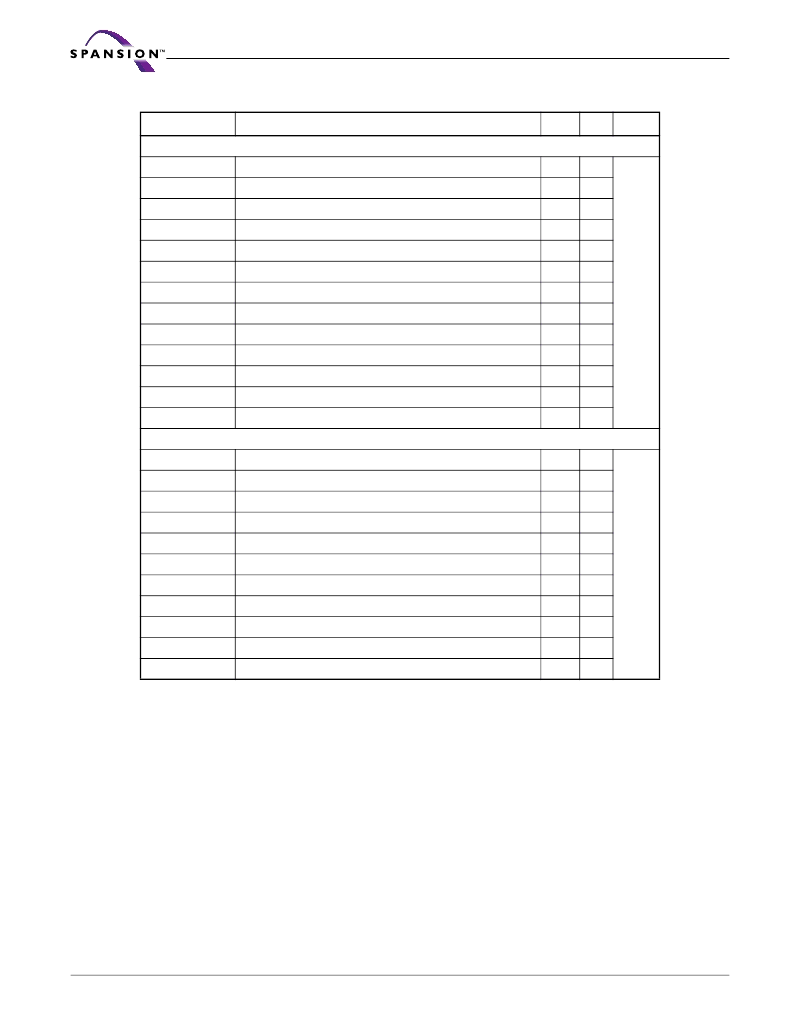
Table 26. Switching Characteristics
Notes:
1.
Test conditions assume signal transition time of 1V/ns or higher, timing reference levels of V
CC(typ.)
/2, input pulse levels of
0 to V
CC(typ.)
, and output loading of the specified I
OL
/I
OH
and 30 pF load capacitance.
t
HZOE
, t
HZCE
, t
HZBE
and t
HZWE
transitions are measured when the outputs enter a high-impedance state.
2.
3.
High-Z and Low-Z parameters are characterized and are not 100% tested.
4.
To achieve 55-ns performance, the read access should be CE# controlled. In this case t
ACE
is the critical parameter and t
SK
is
satisfied when the addresses are stable prior to chip enable going active. For the 70-ns cycle, the addresses must be stable
within 10 ns after the start of the read cycle.
5.
The internal write time of the memory is defined by the overlap of WE#, CE#1 = V
IL
, CE2 = V
IH
, B
HE
and/or B
LE
= V
IL
. All
signals must be Active to initiate a write and any of these signals can terminate a write by going Inactive. The data input set-
up and hold timing should be referenced to the edge of the signal that terminates write.
Parameter
Description
Min
Max
Unit
Read Cycle
t
RC
Read Cycle Time
70
ns
t
AA
Address to Data Valid
70
t
OHA
Data Hold from Address Change
10
t
ACE
CE#1 Low and CE2 High to Data Valid
70
t
DOE
OE# Low to Data Valid
35
t
LZOE
OE# Low to Low Z (note 2, 3)
5
t
HZOE
OE# High to High Z (note 2, 3)
25
t
LZCE
CE#1 Low and CE2 High to Low Z (note 2, 3)
5
t
HZCE
CE#1 High and CE2 Low to High Z (note 2, 3)
25
t
DBE
BHE# / BLE# Low to Data Valid
70
t
LZBE
BHE# / BLE# Low to Low Z (note 2, 3)
5
t
HZBE
BHE# / BLE# High to High Z (note 2, 3)
25
t
SK
(note 4)
Address Skew
10
W rite Cycle ( note 5)
t
WC
Write Cycle Time
70
ns
t
SCE
CE#1 Low an CE2 High to Write End
55
t
AW
Address Set-Up to Write End
55
t
HA
Address Hold from Write End
0
t
SA
Address Set-Up to Write Start
0
t
PWE
WE# Pulse Width
55
t
BW
BLE# / BHE# LOW to Write End
55
t
SD
Data Set-up to Write End
25
t
HD
Data Hold from Write End
0
t
HZWE
WE# Low to High Z (note 2, 3)
25
t
LZWE
WE# High to Low Z (note 2, 3)
5
相關(guān)PDF資料 |
PDF描述 |
|---|---|
| S71GL064A80BAW0B3 | Stacked Multi-Chip Product (MCP) Flash Memory and RAM |
| S71GL064A80BAW0F3 | Stacked Multi-Chip Product (MCP) Flash Memory and RAM |
| S71GL064A80BFI0B0 | Stacked Multi-Chip Product (MCP) Flash Memory and RAM |
| S71GL064A80BFI0B2 | INDUCTOR POWER 3.3UH 5.4A SMD |
| S71GL064A80BFI0B3 | Stacked Multi-Chip Product (MCP) Flash Memory and RAM |
相關(guān)代理商/技術(shù)參數(shù) |
參數(shù)描述 |
|---|---|
| S71GL064A80BAW0B0 | 制造商:SPANSION 制造商全稱:SPANSION 功能描述:Stacked Multi-Chip Product (MCP) Flash Memory and RAM |
| S71GL064A80BAW0B2 | 制造商:SPANSION 制造商全稱:SPANSION 功能描述:Stacked Multi-Chip Product (MCP) Flash Memory and RAM |
| S71GL064A80BAW0B3 | 制造商:SPANSION 制造商全稱:SPANSION 功能描述:Stacked Multi-Chip Product (MCP) Flash Memory and RAM |
| S71GL064A80BAW0F0 | 制造商:SPANSION 制造商全稱:SPANSION 功能描述:Stacked Multi-Chip Product (MCP) Flash Memory and RAM |
| S71GL064A80BAW0F2 | 制造商:SPANSION 制造商全稱:SPANSION 功能描述:Stacked Multi-Chip Product (MCP) Flash Memory and RAM |
發(fā)布緊急采購(gòu),3分鐘左右您將得到回復(fù)。