- 您現(xiàn)在的位置:買賣IC網(wǎng) > PDF目錄374647 > S2076 (Applied Micro Circuits Corp.) Quad Fibre Channel Transceiver(四光纖通道收發(fā)器) PDF資料下載
第1頁第2頁第3頁第4頁當(dāng)前第5頁第6頁第7頁第8頁第9頁第10頁第11頁第12頁第13頁第14頁第15頁第16頁第17頁第18頁第19頁第20頁第21頁第22頁第23頁第24頁第25頁第26頁第27頁第28頁
5
S2076
QUAD FIBRE CHANNEL TRANSCEIVER
October 13, 2000 / Revision B
TRANSMITTER DESCRIPTION
The transmitter section of the S2076 contains a
single PLL which is used to generate the serial rate
transmit clock for all transmitters. Transmitter
functionalities are shown schematically in Figure 3.
Four channels are provided with a variety of options
regarding input clocking and loopback. The transmit-
ters operate at 1.062 GHz, 10 or 20 times the refer-
ence clock frequency.
Data Input
The S2076 has been designed to simplify the paral-
lel interface data transfer and provides flexibility in
the clocking of parallel data. Prior implementations
of this function have either forced the user to syn-
chronize transmit data to the reference clock or to
provide the output clock as a reference to the PLL,
resulting in increased jitter at the serial interface.
The S2076 incorporates a unique FIFO structure
which enables the user to provide a “clean” refer-
ence source for the PLL and to accept a separate
external clock which is used exclusively to reliably
clock data into the device.
The S2076 also provides a system clock output,
TCLKO, which is derived from the internal VCO. The
frequency of this output is constant at the parallel
word rate, 1/10 the serial data rate, regardless of
whether the reference is provided at 1/10 or 1/20 the
serial data rate. This clock can be used by upstream
circuitry as a system clock. See Table 2.
Data to be input to the S2076 should be coded to
insure transition density and DC balance. Data is
input to each channel of the S2076 as a 10 bit wide
word. An input FIFO and a clock input,
TBCx, are
provided for each channel of the S2076. The device
can operate in two different modes. The S2076 can
be configured to use either the TBCx (TBC MODE)
input or the REFCLK input (REFCLK MODE). Table
1 provides a summary of the input modes for the
S2076.
Operation in the TBC MODE makes it easier for us-
ers to meet the relatively narrow setup and hold time
window required by the parallel 10-bit interface. The
TBC signal is used to clock the data into an internal
holding register and the S2076 synchronizes its in-
ternal data flow to insure stable operation. REFCLK,
not TBCx, is used as the reference for the DIN PLL.
This insures minimum jitter on the high speed serial
data stream.
The TBC must be frequency locked to
REFCLK, but
may have an arbitrary but fixed phase relationship.
Adjustment of internal timing of the S2076 is per-
formed during reset. Once synchronized, the S2076
can tolerate up to
±
3ns of phase drift between TBC
and REFCLK.
E
D
O
M
T
n
o
r
e
p
O
0
.
n
n
a
h
c
l
r
d
e
s
u
K
L
C
F
E
R
.
d
o
M
K
L
C
F
E
R
1
l
o
a
d
k
c
o
o
d
e
s
u
x
C
B
T
.
d
o
M
.
O
C
B
T
F
E
T
A
R
L
E
S
K
L
C
K
c
L
n
C
e
u
F
E
q
e
R
r
y
F
t
u
p
t
u
O
l
e
S
e
R
0
K
q
L
e
r
C
F
T
0
0
0
1
R
D
S
s
p
b
M
5
6
0
1
0
1
R
D
S
0
1
0
2
R
D
S
s
p
b
M
5
6
0
1
0
1
R
D
S
1
0
0
1
R
D
S
s
p
b
M
5
2
3
5
0
1
R
D
S
1
1
0
2
R
D
S
s
p
b
M
5
2
3
5
0
1
R
D
S
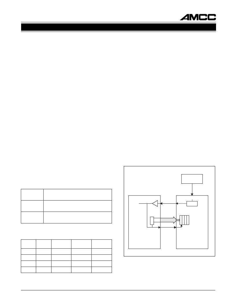
Table 1. Input Modes
Table 2. Operating Rates
REFCLK
S2076
106.25 MHz or 53.125 MHz
TBCx
DINx[0:9]
REF
OSCILLATOR
MAC
ASIC
TCLKO
PLL
Figure 5. DIN Clocking with TBC
Note that internal synchronization of FIFOs is performed upon
de-assertion of RESET.
Note: SDR = Serial Data Rate.
相關(guān)PDF資料 |
PDF描述 |
|---|---|
| S2078 | Dual Fibre Channel Transceiver(雙光纖通道收發(fā)器) |
| S2080 | 34×34 3.2 Gbit/s Differential Crosspoint Switch(高達(dá)3.2 Gbit/s數(shù)據(jù)傳送速率的34×34差分交叉開關(guān)) |
| S208T01 | Low Profile Type Solid State Relays |
| S208T02 | Low Profile Type Solid State Relays |
| S2091 | 2.5 Gbit Port Bypass Circuit for Fibre Channel Arbitrated Loop(用于光纖通道仲裁環(huán)路的端口旁路電路) |
相關(guān)代理商/技術(shù)參數(shù) |
參數(shù)描述 |
|---|---|
| S2079 | 制造商:MA-COM 制造商全稱:M/A-COM Technology Solutions, Inc. 功能描述:Drivers for GaAs FET Switches and Digital Attenuators |
| S2079B1LF | 制造商:BOTHHAND 制造商全稱:Bothhand USA, LP. 功能描述:ISDN S-INTERFACE DUAL TRANSFORMER MODULES SMLL SMT PACKAGE 23.5×12.3×9mm |
| S207R | 制造商:MINMAX 制造商全稱:Minmax Technology Co., Ltd. 功能描述:2W, Low Cost DIP, Single & Dual Output DC/DC Converters |
| S-208 | 制造商:SCANBE/VERO 功能描述: |
| S2080 | 制造商:Tyan 功能描述:MB;ATX;S370;PIIIT;SDRAM;SINGLE 制造商:Microsemi Corporation 功能描述:800V 16A 2PIN DO-203AA - Bulk |
發(fā)布緊急采購,3分鐘左右您將得到回復(fù)。