- 您現(xiàn)在的位置:買賣IC網(wǎng) > PDF目錄98068 > S1C63653F 4-BIT, FLASH, 4 MHz, MICROCONTROLLER, CQFP100 PDF資料下載
參數(shù)資料
| 型號: | S1C63653F |
| 元件分類: | 微控制器/微處理器 |
| 英文描述: | 4-BIT, FLASH, 4 MHz, MICROCONTROLLER, CQFP100 |
| 封裝: | CERAMIC, QFP15-100 |
| 文件頁數(shù): | 116/121頁 |
| 文件大小: | 1127K |
| 代理商: | S1C63653F |
第1頁第2頁第3頁第4頁第5頁第6頁第7頁第8頁第9頁第10頁第11頁第12頁第13頁第14頁第15頁第16頁第17頁第18頁第19頁第20頁第21頁第22頁第23頁第24頁第25頁第26頁第27頁第28頁第29頁第30頁第31頁第32頁第33頁第34頁第35頁第36頁第37頁第38頁第39頁第40頁第41頁第42頁第43頁第44頁第45頁第46頁第47頁第48頁第49頁第50頁第51頁第52頁第53頁第54頁第55頁第56頁第57頁第58頁第59頁第60頁第61頁第62頁第63頁第64頁第65頁第66頁第67頁第68頁第69頁第70頁第71頁第72頁第73頁第74頁第75頁第76頁第77頁第78頁第79頁第80頁第81頁第82頁第83頁第84頁第85頁第86頁第87頁第88頁第89頁第90頁第91頁第92頁第93頁第94頁第95頁第96頁第97頁第98頁第99頁第100頁第101頁第102頁第103頁第104頁第105頁第106頁第107頁第108頁第109頁第110頁第111頁第112頁第113頁第114頁第115頁當前第116頁第117頁第118頁第119頁第120頁第121頁
86
EPSON
S1C63653 TECHNICAL MANUAL
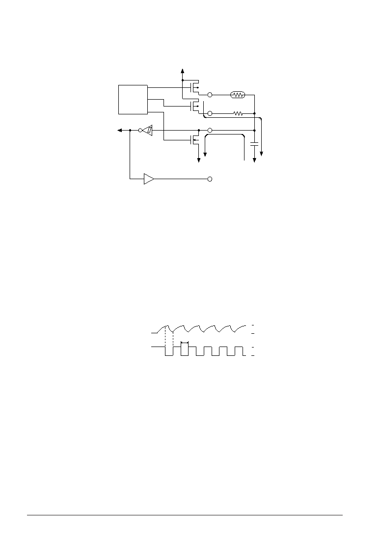
CHAPTER 4: PERIPHERAL CIRCUITS AND OPERATION (R/f Converter)
The CR oscillation circuit is designed so that either the reference resistance side or the sensor side can
be operated independently by the oscillation control circuit.
Each circuit performs the same oscillating operation as follows:
VSS
Tr2
Tr1
Tr3
VSS
SEN0(1)
REF0(1)
RFIN0(1)
VDD
Oscillation
control
circuit
RFOUT
Count
clock
Fig. 4.12.2.2 CR oscillation circuit (DC bias)
The Tr1 (Tr2) turns on first, and the capacitor connected between the REF (SEN) and VSS terminals is
charged through the reference resistance (sensor). If the voltage level of the RFIN terminal decreases,
the Tr1 (Tr2) turns off and the Tr3 turns on. As a result, the capacitor becomes discharged, and oscilla-
tion is performed according to CR time constant. The time constant changes as the sensor resistance
value fluctuates, producing a difference from the oscillation frequency of the reference resistance.
Oscillation waveforms are shaped by the schmitt trigger and transmitted to the measurement counter.
The clock transmitted to the measurement counter is also output from the RFOUT terminal while the
sensor is oscillating. As a result, oscillation frequency can be identified by the oscilloscope. Since this
monitor has no effect on oscillation frequency, it can be used to adjust R/f conversion accuracy.
Oscillation waveforms and waveforms output from the RFOUT terminal are shown in Figure 4.12.2.3.
The "L" pulse width of the RFOUT output must be 10 sec or more (when VDD = 3.0 V, RSEN0/1 = 50
k
, CRF = 1000 pF).
RFIN0/1 terminal
RFOUT output
VDD
VSS
VDD
VSS
10
sec or more
Fig. 4.12.2.3 Oscillation waveform
相關PDF資料 |
PDF描述 |
|---|---|
| S1C6F567D0A0100 | MICROCONTROLLER, UUC141 |
| S1C6N3B0D0A0100 | MICROCONTROLLER, UUC54 |
| S1C6P366D0A0100 | 4-BIT, FLASH, 4.1 MHz, MICROCONTROLLER, UUC102 |
| S1C6P466D0A0A00 | MICROCONTROLLER, UUC140 |
| S1C6S2L7D | 4-BIT, MROM, 0.032 MHz, MICROCONTROLLER, UUC58 |
相關代理商/技術參數(shù) |
參數(shù)描述 |
|---|---|
| S1C63656 | 制造商:EPSON 制造商全稱:EPSON 功能描述:4-bit Single Chip Microcomputer |
| S1C63657 | 制造商:EPSON 制造商全稱:EPSON 功能描述:CMOS 4-bit Single Chip Microcontroller |
| S1C63658 | 制造商:EPSON 制造商全稱:EPSON 功能描述:4-bit Single Chip Microcomputer |
| S1C63666 | 制造商:EPSON 制造商全稱:EPSON 功能描述:4-bit Single Chip Microcomputer |
| S1C63709 | 制造商:EPSON 制造商全稱:EPSON 功能描述:4-bit Single Chip Microcomputer |
發(fā)布緊急采購,3分鐘左右您將得到回復。