- 您現(xiàn)在的位置:買賣IC網(wǎng) > PDF目錄1966 > QLX4600SIQSR (Intersil)IC EQUALIZER REC 6.25GBPS 46QFN PDF資料下載
參數(shù)資料
| 型號(hào): | QLX4600SIQSR |
| 廠商: | Intersil |
| 文件頁(yè)數(shù): | 9/23頁(yè) |
| 文件大小: | 0K |
| 描述: | IC EQUALIZER REC 6.25GBPS 46QFN |
| 標(biāo)準(zhǔn)包裝: | 100 |
| 系列: | QLx™ |
| 應(yīng)用: | 銅電纜模塊 |
| 電源電壓: | 1.1 V ~ 1.3 V |
| 封裝/外殼: | 46-WFQFN 裸露焊盤 |
| 供應(yīng)商設(shè)備封裝: | 46-TQFN |
| 包裝: | 帶卷 (TR) |
| 安裝類型: | 表面貼裝 |
第1頁(yè)第2頁(yè)第3頁(yè)第4頁(yè)第5頁(yè)第6頁(yè)第7頁(yè)第8頁(yè)當(dāng)前第9頁(yè)第10頁(yè)第11頁(yè)第12頁(yè)第13頁(yè)第14頁(yè)第15頁(yè)第16頁(yè)第17頁(yè)第18頁(yè)第19頁(yè)第20頁(yè)第21頁(yè)第22頁(yè)第23頁(yè)
17
FN6979.1
November 19, 2009
Programming Multiple QLx4600-S30
Devices
The serial bus interface provides a simple means of
setting the equalizer boost levels with a minimal amount
of board circuitry. Many of the serial interface signals can
be shared among the QLx4600-S30 devices on a board
and two options are presented in this section. The first
uses common clock and serial data signals along with
separate ENB signals to select which QLx4600-S30
accepts the programmed changes. The second method
uses a common ENB signal as the serial data is
carried-over from one QLx4600-S30 to the next.
Separate ENB Signals
Multiple QLx4600-S30 devices can be programmed from
a common serial data stream as shown in Figure 28.
Here, each QLx4600-S30 is provided its own ENB signal,
and only one of these ENB signals is pulled ‘LOW’, and
hence accepting the register data, at a time. In this
situation, the programming of each equalizer follows the
steps outlined in Figure 29.
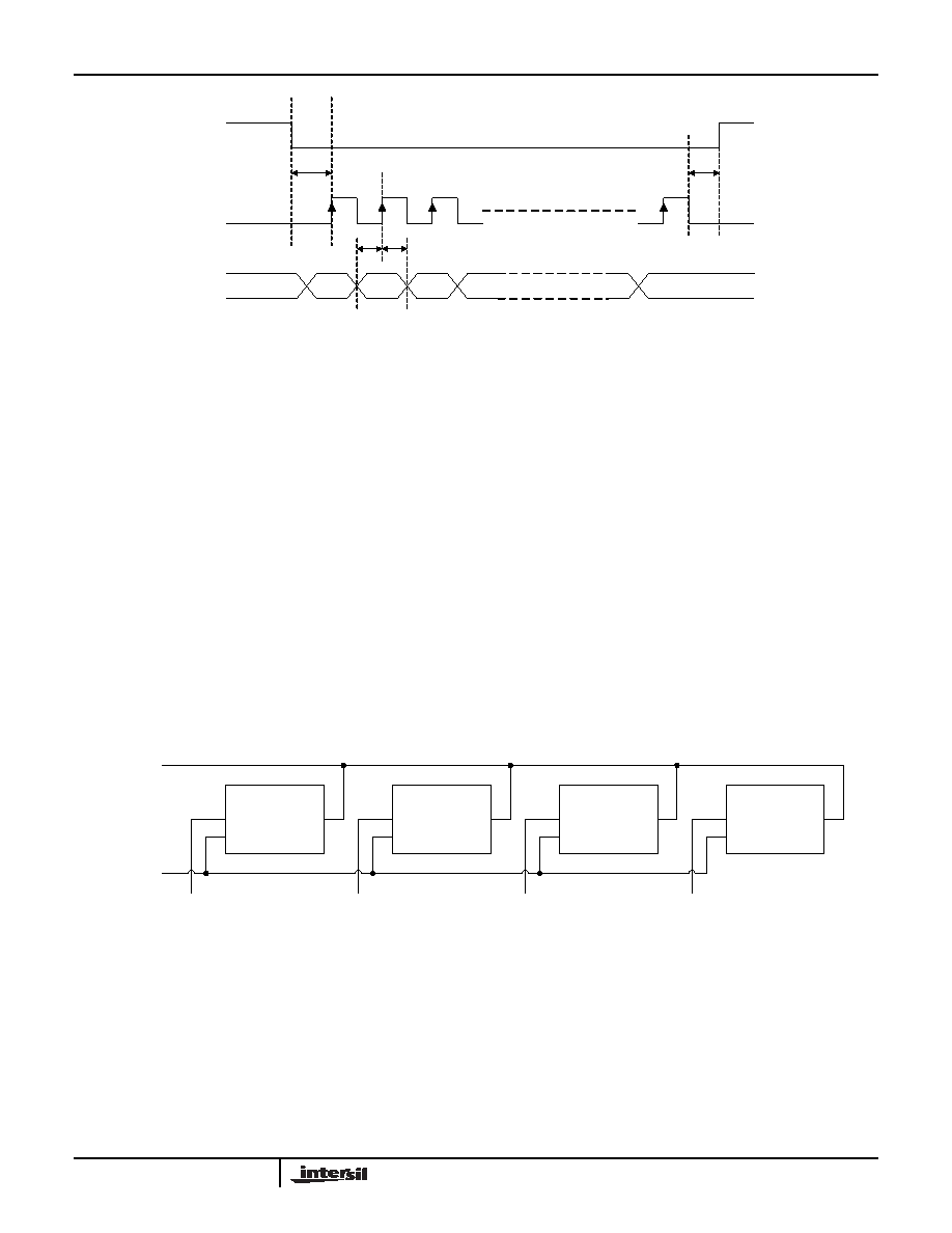
DI/DO Carryover
The DO pin (pin 17) can be used to daisy-chain the serial
bus among multiple QLx4600-S30 chips. The DO pin
outputs the overflow data from the DI pin. Specifically, as
data is pipelined into a QLx4600-S30, it proceeds
according to the following flow. First, a bit goes into
shadow register 1. Then, with each clock cycle, it shifts
over into subsequent higher numbered registers. After
shifting into register 21, it is output on the DO pin on the
same clock cycle. Thus, the DO signal is equal to the DI
signal, but delayed by 20 clock cycles. The timing
diagram for the DO pin is shown in Figure 27 where the
first 20 bits output from the DO are indefinite and
subsequent bits are the data fed into the DI pin. The
delay between the rising clock edge and the data
transition is tCQ.
A diagram for programming multiple QLx4600-S30s is
shown in Figure 30. It is noted that the board layout
should ensure that the additional clock delay experienced
between subsequent QLx4600-S30s should be no more
than the minimum value of tCQ, i.e. 12ns.
R21
R20
R19
R1
tSDI tHDI
tSCK
tHEN
DI
CLK
ENB
FIGURE 27. TIMING DIAGRAM FOR PROGRAMMING THE INTERNAL REGISTERS OF THE QLx4600-S30
QLx4600-S30
(A)
ENB
CLK
DI
DO
QLx4600-S30
(B)
ENB
CLK
DI
DO
QLx4600-S30
(C)
ENB
CLK
DI
DO
QLx4600-S30
(D)
ENB
CLK
DI
DO
ENB (A)
ENB (B)
ENB (C)
ENB (D)
Clock
Serial
Register
Data
FIGURE 28. SERIAL BUS PROGRAMMING MULTIPLE QLx4600-S30 DEVICES USING SEPARATE ENB SIGNALS
QLx4600-S30
相關(guān)PDF資料 |
PDF描述 |
|---|---|
| R5F100GEAFB#V0 | MCU 16BIT 64KB FLASH 48LQFP |
| R5F2135CMNFP#V0 | IC MICROCONTROLLER |
| R5F562N8ADBG#U0 | MCU 32BIT FLASH 512KROM 176LFBGA |
| R5F5630ADDFB#V0 | MCU RX630 768KB FLASH 144-LQFP |
| R5F72167GDFA#V0 | MCU 1MB FLASH 128K 176-LQFP |
相關(guān)代理商/技術(shù)參數(shù) |
參數(shù)描述 |
|---|---|
| QLX4600SIQT7 | 功能描述:接口 - 專用 6 GBS QD CH LANE EXTENDER RoHS:否 制造商:Texas Instruments 產(chǎn)品類型:1080p60 Image Sensor Receiver 工作電源電壓:1.8 V 電源電流:89 mA 最大功率耗散: 最大工作溫度:+ 85 C 安裝風(fēng)格:SMD/SMT 封裝 / 箱體:BGA-59 |
| QLX4600-SL30 | 制造商:INTERSIL 制造商全稱:Intersil Corporation 功能描述:Quad Lane Extender |
| QLZ06 0012-2513 | 制造商:ebm-papst Inc 功能描述: |
| QLZ06 0018-2518 | 制造商:ebm-papst Inc 功能描述: |
| QLZ06 0600-2513 | 制造商:Ebm-Papst Industries 功能描述:Bulk |
發(fā)布緊急采購(gòu),3分鐘左右您將得到回復(fù)。