- 您現(xiàn)在的位置:買賣IC網(wǎng) > PDF目錄299771 > PIC16LC556-04/SS 8-BIT, OTPROM, 4 MHz, RISC MICROCONTROLLER, PDSO20 PDF資料下載
參數(shù)資料
| 型號(hào): | PIC16LC556-04/SS |
| 元件分類: | 微控制器/微處理器 |
| 英文描述: | 8-BIT, OTPROM, 4 MHz, RISC MICROCONTROLLER, PDSO20 |
| 封裝: | 0.209 INCH, PLASTIC, SSOP-20 |
| 文件頁數(shù): | 69/104頁 |
| 文件大小: | 697K |
| 代理商: | PIC16LC556-04/SS |
第1頁第2頁第3頁第4頁第5頁第6頁第7頁第8頁第9頁第10頁第11頁第12頁第13頁第14頁第15頁第16頁第17頁第18頁第19頁第20頁第21頁第22頁第23頁第24頁第25頁第26頁第27頁第28頁第29頁第30頁第31頁第32頁第33頁第34頁第35頁第36頁第37頁第38頁第39頁第40頁第41頁第42頁第43頁第44頁第45頁第46頁第47頁第48頁第49頁第50頁第51頁第52頁第53頁第54頁第55頁第56頁第57頁第58頁第59頁第60頁第61頁第62頁第63頁第64頁第65頁第66頁第67頁第68頁當(dāng)前第69頁第70頁第71頁第72頁第73頁第74頁第75頁第76頁第77頁第78頁第79頁第80頁第81頁第82頁第83頁第84頁第85頁第86頁第87頁第88頁第89頁第90頁第91頁第92頁第93頁第94頁第95頁第96頁第97頁第98頁第99頁第100頁第101頁第102頁第103頁第104頁
1996 Microchip Technology Inc.
Preliminary
DS40143A-page 67
PIC16C55X
10.0
ELECTRICAL SPECIFICATIONS
Absolute Maximum Ratings
Ambient Temperature under bias ............................................................................................................. –40
° to +125°C
Storage Temperature ............................................................................................................................... –65
° to +150°C
Voltage on any pin with respect to VSS (except VDD and MCLR) ......................................................–0.6V to VDD +0.6V
Voltage on VDD with respect to VSS ................................................................................................................ 0 to +7.5V
Voltage on MCLR with respect to VSS (Note 2) .................................................................................................0 to +14V
Total power Dissipation (Note 1) ...............................................................................................................................1.0W
Maximum Current out of VSS pin ..........................................................................................................................300 mA
Maximum Current into VDD pin .............................................................................................................................250 mA
Input Clamp Current, IIK (VI<0 or VI> VDD)
........................................................................................................................±20 mA
Output Clamp Current, IOK (V0 <0 or V0>VDD)
................................................................................................................±20 mA
Maximum Output Current sunk by any I/O pin ........................................................................................................25 mA
Maximum Output Current sourced by any I/O pin...................................................................................................25 mA
Maximum Current sunk by PORTA and PORTB ...................................................................................................200 mA
Maximum Current sourced by PORTA and PORTB..............................................................................................200 mA
Note 1: Power dissipation is calculated as follows: PDIS = VDD x {IDD -
∑ IOH} + ∑ {(VDD-VOH) x IOH} + ∑(VOl x IOL)
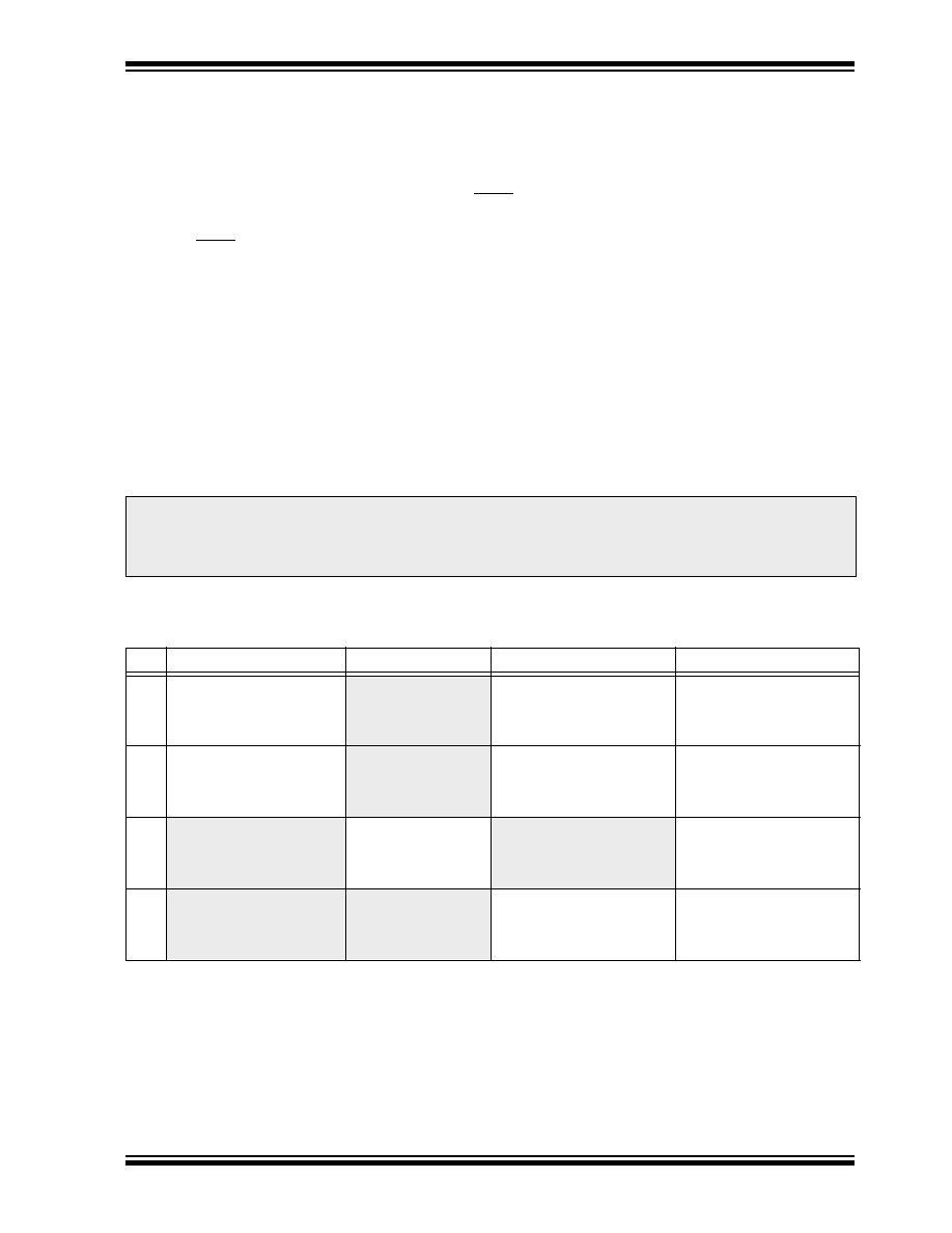
TABLE 10-1:
CROSS REFERENCE OF DEVICE SPECS FOR OSCILLATOR CONFIGURATIONS
AND FREQUENCIES OF OPERATION (COMMERCIAL DEVICES)
NOTICE: Stresses above those listed under "Absolute Maximum Ratings" may cause permanent damage to the
device. This is a stress rating only and functional operation of the device at those or any other conditions above
those indicated in the operation listings of this specication is not implied. Exposure to maximum rating conditions
for extended periods may affect device reliability.
OSC
PIC16C55X-04
PIC16C55X-20
PIC16LC55X-04
JW Devices
RC
VDD: 3.0V to 5.5V
IDD: 3.3 mA max. @5.5V
IPD: 20
A max. @4.0V
Freq: 4.0 MHz max.
VDD: 4.5V to 5.5V
IDD: 1.8 mA typ. @5.5V
IPD: 1.0
A typ. @4.5V
Freq: 4.0 MHz max.
VDD: 2.5V to 5.5V
IDD: 1.4 mA typ. @3.0V
IPD: 0.7
A typ. @3.0V
Freq: 4.0 MHz max.
VDD: 3.0V to 5.5V
IDD: 3.3 mA max. @5.5V
IPD: 20
A max. @4.0V
Freq: 4.0 MHz Max.
XT
VDD: 3.0V to 5.5V
IDD: 3.3 mA max. @5.5V
IPD: 20
A max. @4.0V
Freq: 4.0 MHz max.
VDD: 4.5V to 5.5V
IDD: 1.8 mA typ. @5.5V
IPD: 1.0
A typ. @4.5V
Freq: 4.0 MHz max.
VDD: 2.5V to 5.5V
IDD: 1.4 mA typ. @3.0V
IPD: 0.7
A typ. @3.0V
Freq: 4.0 MHz max.
VDD: 3.0V to 5.5V
IDD: 3.3 mA max. @5.5V
IPD: 20
A max. @4.0V
Freq: 4.0 MHz max.
HS
VDD: 4.5V to 5.5V
IDD: 9.0 mA typ. @5.5V
IPD: 1.0
A typ. @4.0V
Freq: 4.0 MHz max.
VDD: 4.5V to 5.5V
IDD: 20 mA max. @5.5V
IPD: 1.0
A typ. @4.5V
Freq: 20 MHz max.
Do not use in HS mode
VDD: 4.5V to 5.5V
IDD: 20 mA max. @5.5V
IPD: 1.0
A typ. @4.5V
Freq: 20 MHz max.
LP
VDD: 3.0V to 5.5V
IDD: 35
A typ. @32 kHz, 3.0V
IPD: 1.0
A typ. @4.0 V
Freq: 200 kHz maximum
Do not use in LP mode
VDD: 2.5V to 5.5V
IDD: 32
A max. @32 kHz, 3.0V
IPD: 9.0
A max. @3.0V
Freq: 200 kHz max.
VDD: 2.5V to 5.5V
IDD: 32
A max. @32 kHz, 3.0V
IPD: 9.0
A Max. @3.0V
Freq: 200 kHz max.
The shaded sections indicate oscillator selections which are tested for functionality, but not for MIN/MAX specications. It is recom-
mended that the user select the device type that guarantees the specications required.
This document was created with FrameMaker404
相關(guān)PDF資料 |
PDF描述 |
|---|---|
| PIC16LC662T-04/L | 8-BIT, OTPROM, 4 MHz, RISC MICROCONTROLLER, PQCC44 |
| PIC16C662T-20I/P | 8-BIT, OTPROM, 20 MHz, RISC MICROCONTROLLER, PDIP40 |
| PIC16C662T-20I/L | 8-BIT, OTPROM, 20 MHz, RISC MICROCONTROLLER, PQCC44 |
| PIC16C662T-04E/TQ | 8-BIT, OTPROM, 4 MHz, RISC MICROCONTROLLER, PQFP44 |
| PIC16LC715T-04/SS | 8-BIT, OTPROM, 4 MHz, RISC MICROCONTROLLER, PDSO20 |
相關(guān)代理商/技術(shù)參數(shù) |
參數(shù)描述 |
|---|---|
| PIC16LC558-04/P | 功能描述:8位微控制器 -MCU 3.5KB 128 RAM 13 I/O RoHS:否 制造商:Silicon Labs 核心:8051 處理器系列:C8051F39x 數(shù)據(jù)總線寬度:8 bit 最大時(shí)鐘頻率:50 MHz 程序存儲(chǔ)器大小:16 KB 數(shù)據(jù) RAM 大小:1 KB 片上 ADC:Yes 工作電源電壓:1.8 V to 3.6 V 工作溫度范圍:- 40 C to + 105 C 封裝 / 箱體:QFN-20 安裝風(fēng)格:SMD/SMT |
| PIC16LC558-04/SO | 功能描述:8位微控制器 -MCU 3.5KB 128 RAM 13 I/O RoHS:否 制造商:Silicon Labs 核心:8051 處理器系列:C8051F39x 數(shù)據(jù)總線寬度:8 bit 最大時(shí)鐘頻率:50 MHz 程序存儲(chǔ)器大小:16 KB 數(shù)據(jù) RAM 大小:1 KB 片上 ADC:Yes 工作電源電壓:1.8 V to 3.6 V 工作溫度范圍:- 40 C to + 105 C 封裝 / 箱體:QFN-20 安裝風(fēng)格:SMD/SMT |
| PIC16LC558-04/SS | 功能描述:8位微控制器 -MCU 3.5KB 128 RAM 13 I/O RoHS:否 制造商:Silicon Labs 核心:8051 處理器系列:C8051F39x 數(shù)據(jù)總線寬度:8 bit 最大時(shí)鐘頻率:50 MHz 程序存儲(chǔ)器大小:16 KB 數(shù)據(jù) RAM 大小:1 KB 片上 ADC:Yes 工作電源電壓:1.8 V to 3.6 V 工作溫度范圍:- 40 C to + 105 C 封裝 / 箱體:QFN-20 安裝風(fēng)格:SMD/SMT |
| PIC16LC558-04E/P | 功能描述:8位微控制器 -MCU 3.5KB 128 RAM 13 I/O RoHS:否 制造商:Silicon Labs 核心:8051 處理器系列:C8051F39x 數(shù)據(jù)總線寬度:8 bit 最大時(shí)鐘頻率:50 MHz 程序存儲(chǔ)器大小:16 KB 數(shù)據(jù) RAM 大小:1 KB 片上 ADC:Yes 工作電源電壓:1.8 V to 3.6 V 工作溫度范圍:- 40 C to + 105 C 封裝 / 箱體:QFN-20 安裝風(fēng)格:SMD/SMT |
| PIC16LC558-04E/SO | 功能描述:8位微控制器 -MCU 3.5KB 128 RAM 13 I/O RoHS:否 制造商:Silicon Labs 核心:8051 處理器系列:C8051F39x 數(shù)據(jù)總線寬度:8 bit 最大時(shí)鐘頻率:50 MHz 程序存儲(chǔ)器大小:16 KB 數(shù)據(jù) RAM 大小:1 KB 片上 ADC:Yes 工作電源電壓:1.8 V to 3.6 V 工作溫度范圍:- 40 C to + 105 C 封裝 / 箱體:QFN-20 安裝風(fēng)格:SMD/SMT |
發(fā)布緊急采購,3分鐘左右您將得到回復(fù)。