- 您現(xiàn)在的位置:買賣IC網(wǎng) > PDF目錄383714 > OR2T04A-5M208I (Electronic Theatre Controls, Inc.) Field-Programmable Gate Arrays PDF資料下載
參數(shù)資料
| 型號(hào): | OR2T04A-5M208I |
| 廠商: | Electronic Theatre Controls, Inc. |
| 元件分類: | FPGA |
| 英文描述: | Field-Programmable Gate Arrays |
| 中文描述: | 現(xiàn)場(chǎng)可編程門陣列 |
| 文件頁(yè)數(shù): | 47/192頁(yè) |
| 文件大?。?/td> | 3148K |
| 代理商: | OR2T04A-5M208I |
第1頁(yè)第2頁(yè)第3頁(yè)第4頁(yè)第5頁(yè)第6頁(yè)第7頁(yè)第8頁(yè)第9頁(yè)第10頁(yè)第11頁(yè)第12頁(yè)第13頁(yè)第14頁(yè)第15頁(yè)第16頁(yè)第17頁(yè)第18頁(yè)第19頁(yè)第20頁(yè)第21頁(yè)第22頁(yè)第23頁(yè)第24頁(yè)第25頁(yè)第26頁(yè)第27頁(yè)第28頁(yè)第29頁(yè)第30頁(yè)第31頁(yè)第32頁(yè)第33頁(yè)第34頁(yè)第35頁(yè)第36頁(yè)第37頁(yè)第38頁(yè)第39頁(yè)第40頁(yè)第41頁(yè)第42頁(yè)第43頁(yè)第44頁(yè)第45頁(yè)第46頁(yè)當(dāng)前第47頁(yè)第48頁(yè)第49頁(yè)第50頁(yè)第51頁(yè)第52頁(yè)第53頁(yè)第54頁(yè)第55頁(yè)第56頁(yè)第57頁(yè)第58頁(yè)第59頁(yè)第60頁(yè)第61頁(yè)第62頁(yè)第63頁(yè)第64頁(yè)第65頁(yè)第66頁(yè)第67頁(yè)第68頁(yè)第69頁(yè)第70頁(yè)第71頁(yè)第72頁(yè)第73頁(yè)第74頁(yè)第75頁(yè)第76頁(yè)第77頁(yè)第78頁(yè)第79頁(yè)第80頁(yè)第81頁(yè)第82頁(yè)第83頁(yè)第84頁(yè)第85頁(yè)第86頁(yè)第87頁(yè)第88頁(yè)第89頁(yè)第90頁(yè)第91頁(yè)第92頁(yè)第93頁(yè)第94頁(yè)第95頁(yè)第96頁(yè)第97頁(yè)第98頁(yè)第99頁(yè)第100頁(yè)第101頁(yè)第102頁(yè)第103頁(yè)第104頁(yè)第105頁(yè)第106頁(yè)第107頁(yè)第108頁(yè)第109頁(yè)第110頁(yè)第111頁(yè)第112頁(yè)第113頁(yè)第114頁(yè)第115頁(yè)第116頁(yè)第117頁(yè)第118頁(yè)第119頁(yè)第120頁(yè)第121頁(yè)第122頁(yè)第123頁(yè)第124頁(yè)第125頁(yè)第126頁(yè)第127頁(yè)第128頁(yè)第129頁(yè)第130頁(yè)第131頁(yè)第132頁(yè)第133頁(yè)第134頁(yè)第135頁(yè)第136頁(yè)第137頁(yè)第138頁(yè)第139頁(yè)第140頁(yè)第141頁(yè)第142頁(yè)第143頁(yè)第144頁(yè)第145頁(yè)第146頁(yè)第147頁(yè)第148頁(yè)第149頁(yè)第150頁(yè)第151頁(yè)第152頁(yè)第153頁(yè)第154頁(yè)第155頁(yè)第156頁(yè)第157頁(yè)第158頁(yè)第159頁(yè)第160頁(yè)第161頁(yè)第162頁(yè)第163頁(yè)第164頁(yè)第165頁(yè)第166頁(yè)第167頁(yè)第168頁(yè)第169頁(yè)第170頁(yè)第171頁(yè)第172頁(yè)第173頁(yè)第174頁(yè)第175頁(yè)第176頁(yè)第177頁(yè)第178頁(yè)第179頁(yè)第180頁(yè)第181頁(yè)第182頁(yè)第183頁(yè)第184頁(yè)第185頁(yè)第186頁(yè)第187頁(yè)第188頁(yè)第189頁(yè)第190頁(yè)第191頁(yè)第192頁(yè)
Lucent Technologies Inc.
47
Data Sheet
June 1999
ORCA Series 2 FPGAs
Bit Stream Error Checking
There are three different types of bit stream error
checking performed in the ORCA Series 2 FPGAs:
ID frame, frame alignment, and parity checking.
An optional ID data frame can be sent to a specified
address in the FPGA. This ID frame contains a unique
code for the part it was generated for which is com-
pared within the FPGA. Any differences are flagged as
an ID error. This frame is automatically created by the
bit stream generation program in ORCAFoundry.
Every data frame in the FPGA begins with a start bit
set to 0 and three or more stop bits set to 1. If any of
the three previous bits were a 0 when a start bit is
encountered, it is flagged as a frame alignment error.
Parity checking is also done on the FPGA for each
frame, if it has been enabled by setting the prty_en bit
to 1 in the ID frame. This is set by enabling the parity
check option in the bit stream generation program of
ORCA Foundry. Two parity bits, opar and epar, are
used to check the parity of bits in alternating bit posi-
tions to even parity in each data frame. If an odd num-
ber of ones is found for either the even bits (starting
with the start bit) or the odd bits (starting with the pro-
gram bit), then a parity error is flagged.
When any of the three possible errors occur, the FPGA
is forced into the INIT state, forcing
INIT
low. The FPGA
will remain in this state until either the
RESET
or
PRGM
pins are asserted.
FPGA Configuration Modes
There are eight methods for configuring the FPGA.
Seven of the configuration modes are selected on the
M0, M1, and M2 inputs. The eighth configuration mode
is accessed through the boundary-scan interface. A
fourth input, M3, is used to select the frequency of the
internal oscillator, which is the source for CCLK in
some configuration modes. The nominal frequencies of
the internal oscillator are 1.25 MHz and 10 MHz. The
1.25 MHz frequency is selected when the M3 input is
unconnected or driven to a high state.
There are three basic FPGA configuration modes:
master, slave, and peripheral. The configuration data
can be transmitted to the FPGA serially or in parallel
bytes. As a master, the FPGA provides the control sig-
nals out to strobe data in. As a slave device, a clock is
generated externally and provided into CCLK. In the
peripheral mode, the FPGA acts as a microprocessor
peripheral. Table 10 lists the functions of the configura-
tion mode pins.
Table 10. Configuration Modes
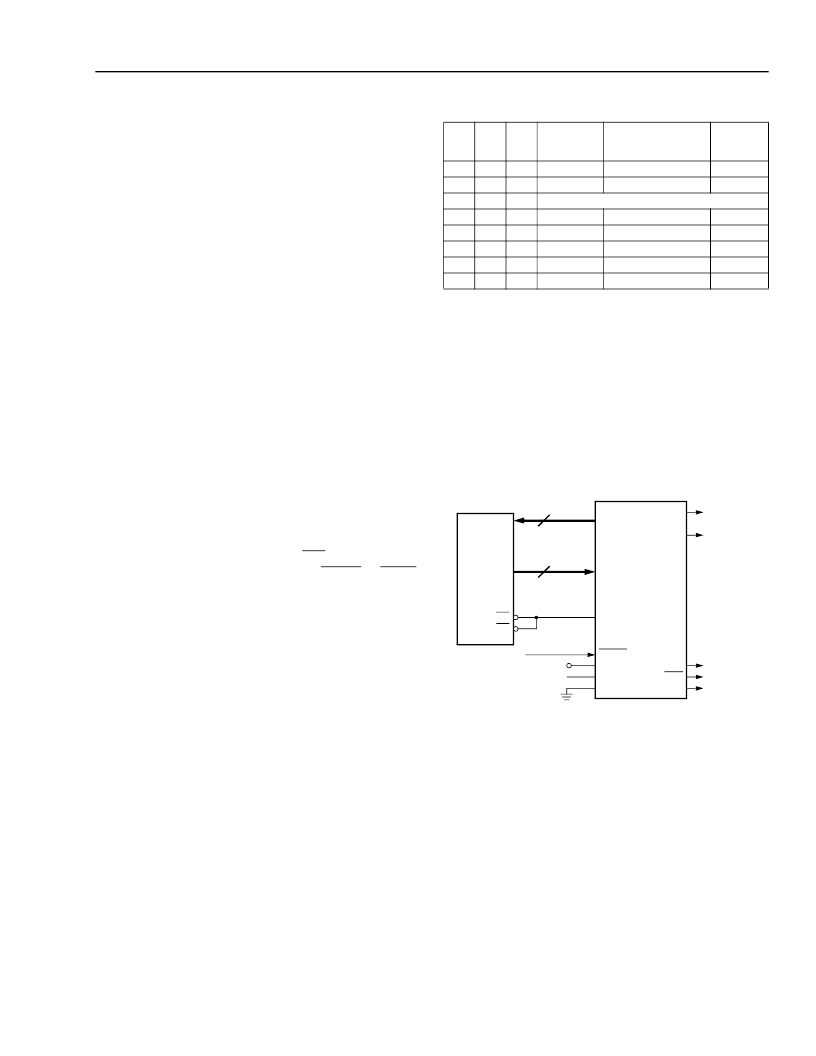
Master Parallel Mode
The master parallel configuration mode is generally
used to interface to industry-standard byte-wide mem-
ory, such as the 2764 and larger EPROMs. Figure 40
provides the connections for master parallel mode. The
FPGA outputs an 18-bit address on A[17:0] to memory
and reads one byte of configuration data on the rising
edge of RCLK. The parallel bytes are internally serial-
ized starting with the least significant bit, D0.
5-4483(F)
Figure 40. Master Parallel Configuration Schematic
There are two parallel master modes: master up and
master down. In master up, the starting memory
address is 00000 Hex and the FPGA increments the
address for each byte loaded. In master down, the
starting memory address is 3FFFF Hex and the FPGA
decrements the address.
One master mode FPGA can interface to the memory
and provide configuration data on DOUT to additional
FPGAs in a daisy chain. The configuration data on
DOUT is provided synchronously with the falling edge
of CCLK. The frequency of the CCLK output is eight
times that of RCLK.
M2
M1
M0
CCLK
Configuration
Mode
Master
Slave Parallel
Data
0
0
0
0
1
1
1
1
0
0
1
1
0
0
1
1
0
1
0
1
0
1
0
1
Output
Input
Reserved
Input
Output
Output
Output
Input
Serial
Parallel
Sync Peripheral
Master (up)
Async Peripheral
Master (down)
Slave
Parallel
Parallel
Parallel
Parallel
Serial
TO DAISY-
CHAINED
DEVICES
DOUT
CCLK
HDC
LDC
RCLK
A[17:0]
D[7:0]
DONE
PRGM
M2
M1
M0
A[17:0]
D[7:0]
OE
CE
PROGRAM
V
DD
V
DD
OR GND
EPROM
ORCA
SERIES
FPGA
相關(guān)PDF資料 |
PDF描述 |
|---|---|
| OR2T04A-5M84 | Field-Programmable Gate Arrays |
| OR2T04A-5M84I | Field-Programmable Gate Arrays |
| OR2T04A-5PS208 | Field-Programmable Gate Arrays |
| OR2T04A-5PS208I | Field-Programmable Gate Arrays |
| OR2T04A-5PS84 | Field-Programmable Gate Arrays |
相關(guān)代理商/技術(shù)參數(shù) |
參數(shù)描述 |
|---|---|
| OR2T04A-5M84 | 制造商:未知廠家 制造商全稱:未知廠家 功能描述:Field-Programmable Gate Arrays |
| OR2T04A-5M84I | 制造商:未知廠家 制造商全稱:未知廠家 功能描述:Field-Programmable Gate Arrays |
| OR2T04A-5PS100 | 制造商:未知廠家 制造商全稱:未知廠家 功能描述:Field-Programmable Gate Arrays |
| OR2T04A-5PS100I | 制造商:未知廠家 制造商全稱:未知廠家 功能描述:Field-Programmable Gate Arrays |
| OR2T04A-5PS144 | 制造商:未知廠家 制造商全稱:未知廠家 功能描述:Field-Programmable Gate Arrays |
發(fā)布緊急采購(gòu),3分鐘左右您將得到回復(fù)。