- 您現(xiàn)在的位置:買賣IC網(wǎng) > PDF目錄383693 > OPA628AU Low Distortion Wideband OPERATIONAL AMPLIFIER PDF資料下載
參數(shù)資料
| 型號: | OPA628AU |
| 英文描述: | Low Distortion Wideband OPERATIONAL AMPLIFIER |
| 中文描述: | 低失真寬帶運(yùn)算放大器 |
| 文件頁數(shù): | 3/13頁 |
| 文件大小: | 172K |
| 代理商: | OPA628AU |
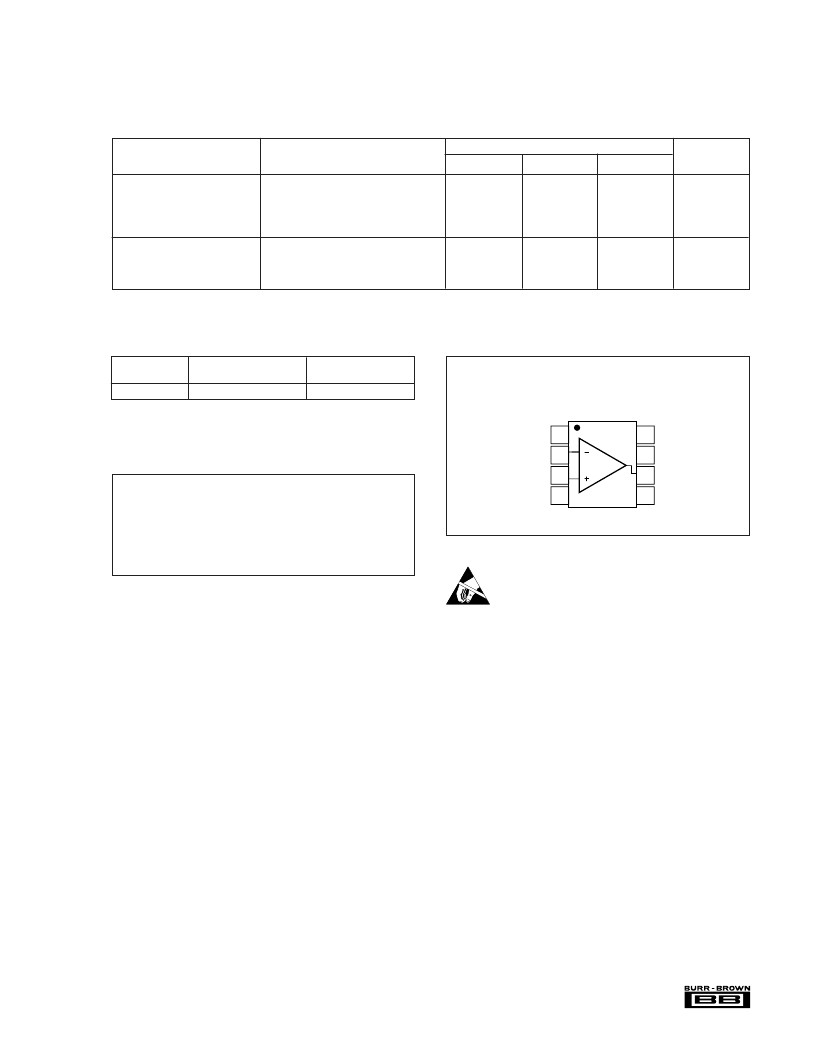
3
OPA628
OPA628
1
2
3
4
5
6
7
8
No Internal Connection
+V
CC
, Output Stage
Inverting Input
Non-Inverting Input
–V
CC
, Input Stage
Output
–V
CC
, Output Stage
+V
CC
, Input Stage
OPA628AU
PARAMETER
CONDITIONS
MIN
TYP
MAX
UNITS
POWER SUPPLY
Rated Voltage
Derated Performance
Current, Quiescent
Current, Quiescent
±
V
CC
±
V
±
5
VDC
VDC
mA
mA
±
4.5
±
6
32
35
I
= 0mADC
29
31
I
O
= 0mADC, T
A
= T
MIN
to T
MAX
TEMPERATURE RANGE
Specification: AU
Storage:
θ
JA
T
and T
Ambient Temperature
Junction-to-Ambient
–40
–55
+85
+125
°
C
°
C
AU
AU
100
°
C/W
The information provided herein is believed to be reliable; however, BURR-BROWN assumes no responsibility for inaccuracies or omissions. BURR-BROWN assumes
no responsibility for the use of this information, and all use of such information shall be entirely at the user’s own risk. Prices and specifications are subject to change
without notice. No patent rights or licenses to any of the circuits described herein are implied or granted to any third party. BURR-BROWN does not authorize or warrant
any BURR-BROWN product for use in life support devices and/or systems.
SPECIFICATIONS
(CONT)
ELECTRICAL
At V
CC
=
±
5VDC, R
L
=100
, G = +2, and T
A
= +25
°
C, unless otherwise noted.
NOTES: (1) Full power response = slew rate/(2
π
Vpeak). (2) Time for output to resume linear operation after saturation.
PIN CONFIGURATION
Top View
8-Pin Plastic SOIC
PACKAGE DRAWING
NUMBER
(1)
PRODUCT
PACKAGE
OPA628AU
SO-8 Surface Mount
182
NOTE: (1) For detailed drawing and dimension table, please see end of data
sheet, or Appendix C of Burr-Brown IC Data Book.
PACKAGE/ORDERING INFORMATION
ABSOLUTE MAXIMUM RATINGS
Supply ..............................................................................................
±
7VDC
Internal Power Dissipation
(1)
........................ See Applications Information
Differential Input Voltage......................................................................... 5V
Input Voltage Range ..................................... See Applications Information
Storage Temperature Range: AP, AU ............................ –55
°
C to +125
°
C
Lead Temperature (soldering, SOIC 3s) ........................................ +260
°
C
Output Short Circuit to Ground (+25
°
C) ................. Continuous to Ground
Junction Temperature (T
J
) ............................................................. +175
°
C
NOTE: (1) Packages must be derated based on specified
θ
JA
. Maximum T
J
must be observed.
ELECTROSTATIC
DISCHARGE SENSITIVITY
This integrated circuit can be damaged by ESD. Burr-Brown
recommends that all integrated circuits be handled with
appropriate precautions. Failure to observe proper handling
and installation procedures can cause damage.
ESD damage can range from subtle performance degradation
to complete device failure. Precision integrated circuits may
be more susceptible to damage because very small parametric
changes could cause the device not to meet its published
specifications.
相關(guān)PDF資料 |
PDF描述 |
|---|---|
| OPA628 | Low Distortion Wideband OPERATIONAL AMPLIFIER |
| OPA654 | Wide Bandwidth, High Output Current Difet OPERATIONAL AMPLIFIER |
| OPA654AM | Wide Bandwidth, High Output Current Difet OPERATIONAL AMPLIFIER |
| OPA655 | Wideband, Unity Gain Stable, FET-Input OPERATIONAL AMPLIFIER |
| OPA655P | Wideband, Unity Gain Stable, FET-Input OPERATIONAL AMPLIFIER |
相關(guān)代理商/技術(shù)參數(shù) |
參數(shù)描述 |
|---|---|
| OPA628U | 制造商:BB 制造商全稱:BB 功能描述:EVALUATION FIXTURE |
| OPA62K5 | 制造商:TI 制造商全稱:Texas Instruments 功能描述:Wideband, Unity-Gain Stable, FET-Input OPERATIONAL AMPLIFIER |
| OPA631 | 制造商:BB 制造商全稱:BB 功能描述:Low Power, Single-Supply OPERATIONAL AMPLIFIERS TM |
| OPA631/OPA632 | 制造商:BB 制造商全稱:BB 功能描述:OPA631. OPA632 - SpeedPlus Low Power. Single-Supply OPERATIONAL AMPLIFIERS |
| OPA6316 | 制造商:KODENSHI 制造商全稱:KODENSHI KOREA CORP. 功能描述:Orange LED Chip |
發(fā)布緊急采購,3分鐘左右您將得到回復(fù)。