- 您現(xiàn)在的位置:買賣IC網(wǎng) > PDF目錄383693 > OPA628 Low Distortion Wideband OPERATIONAL AMPLIFIER PDF資料下載
參數(shù)資料
| 型號: | OPA628 |
| 英文描述: | Low Distortion Wideband OPERATIONAL AMPLIFIER |
| 中文描述: | 低失真寬帶運(yùn)算放大器 |
| 文件頁數(shù): | 8/13頁 |
| 文件大小: | 172K |
| 代理商: | OPA628 |
8
OPA628
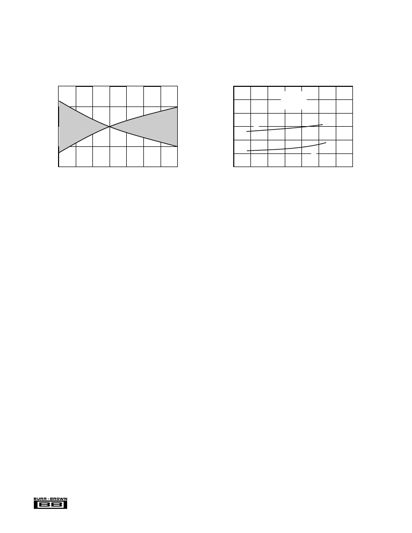
RANGE OF CHANGE IN V
OS
vs TEMPERATURE RELATIVE TO V
OS
at 25°C
1.0
0.5
0
–0.5
–1.0
C
Temperature (°C)
–50
–25
0
25
50
75
100
125
TYPICAL PERFORMANCE CURVES
(CONT)
At V
CC
=
±
5VDC, R
L
=100
, G = +2, and T
A
= +25
°
C, unless otherwise noted.
DISCUSSION OF
PERFORMANCE
The OPA628’s classical operational amplifier architecture
employs true differential and fully symmetrical inputs al-
lowing optimal performance in either inverting or non-
inverting circuit applications. All traditional circuit configu-
rations and op amp theory apply to the OPA628. The use of
low drift thin film resistors allows internal operating cur-
rents to be laser trimmed at wafer level to optimize AC
performance such as distortion, bandwidth and settling time,
as well as DC parameters such as input offset voltage. The
result is a wideband, high frequency monolithic operational
amplifier with a gain-bandwidth product of 150MHz, a
spurious free dynamic range (SFDR) of 90dB, and input
offset voltage of 500
μ
V.
The layout considerations described in the “Printed Circuit
Board Guidelines” section must be followed to achieve the
best possible performance of the OPA628.
DIFFERENTIAL GAIN AND PHASE
Differential Gain (DG) and Differential Phase (DP) are
among the more important specifications for video applica-
tions. DG is defined as the percent change in closed-loop
gain over a specified change in output voltage level. DP is
defined as the change in degrees of the closed-loop phase
over the same output voltage change. Both DG and DP are
specified at the NTSC sub-carrier frequency of 3.58MHz
and the PAL subcarrier of 4.43MHz. All NTSC measure-
ments were performed using a Tektronix model VM700A
Video Measurement Set. All PAL measurements were per-
formed using a Rohde & Schwarz Video Analyzer UAF.
DG and DP of the OPA628 were measured with the ampli-
fier in a gain of +2V/V with 75
input impedance and the
output back-terminated in 75
. The input signal selected
from the generator was a 0V to 1.4V modulated ramp with
sync pulse. With these conditions the test circuit shown in
Figure 1 delivered a 100IRE modulated ramp to the 75
input of the video analyzer. The signal averaging feature of
the analyzer was used to establish a reference against which
the performance of the amplifier was measured. Signal
averaging was also used to measure the DG and DP of the
test signal in order to eliminate the generator’s contribution
to measured amplifier performance. Typical performance of
the OPA628 is 0.015% differential gain and 0.015
°
differen-
tial phase to both NTSC and PAL standards. Increasing the
closed-loop gain degrades the DP and DG.
GAIN FLATNESS
Small signal
±
0.1dB gain flatness can be achieved up to
30MHz in a non-inverting gain of +2V/V through careful
layout of the printed circuit board and frequency shaping of
the feedback network. Frequency shaping is achieved em-
pirically by placing a small capacitor in parallel with either
the feedback resistor or the input resistor of the OPA628 to
compensate for printed circuit parasitic capacitance. A ca-
pacitor in the range of approximately 1pF to 20pF is sug-
gested. Printed circuit board layout design will determine if
the capacitor should be placed across the feedback resistor
or the input resistor.
Small signal
±
0.1dB gain flatness of greater than 30MHz
can be achieved at a gain of +1V/V. To eliminate the effects
of package lead inductance, a small value resistor should be
included in the feedback path. Maximizing gain flatness for
a particular layout requires optimization of the feedback
resistor; an approximate value is 50
to 75
.
DISTORTION
The OPA628’s Harmonic Distortion characteristics when
driving a 100
load are shown vs frequency and vs voltage
output in the Typical Performance Curves. Distortion can be
further optimized by decreasing output loading as also
5MHz HARMONIC DISTORTION vs TEMPERATURE
–70
–75
–80
–85
–90
–95
–100
Temperature (°C)
H
–50
2f
3f
G = +2V/V
V
O
= 2Vp-p
R
L
= 100
–25
0
25
50
75
100
125
相關(guān)PDF資料 |
PDF描述 |
|---|---|
| OPA654 | Wide Bandwidth, High Output Current Difet OPERATIONAL AMPLIFIER |
| OPA654AM | Wide Bandwidth, High Output Current Difet OPERATIONAL AMPLIFIER |
| OPA655 | Wideband, Unity Gain Stable, FET-Input OPERATIONAL AMPLIFIER |
| OPA655P | Wideband, Unity Gain Stable, FET-Input OPERATIONAL AMPLIFIER |
| OPA655U | Wideband, Unity Gain Stable, FET-Input OPERATIONAL AMPLIFIER |
相關(guān)代理商/技術(shù)參數(shù) |
參數(shù)描述 |
|---|---|
| OPA628A WAF | 制造商:Texas Instruments 功能描述: |
| OPA628AP | 制造商:Texas Instruments 功能描述:Part Number Only |
| OPA628AU | 制造商:Rochester Electronics LLC 功能描述:- Bulk |
| OPA628U | 制造商:BB 制造商全稱:BB 功能描述:EVALUATION FIXTURE |
| OPA62K5 | 制造商:TI 制造商全稱:Texas Instruments 功能描述:Wideband, Unity-Gain Stable, FET-Input OPERATIONAL AMPLIFIER |
發(fā)布緊急采購,3分鐘左右您將得到回復(fù)。