- 您現(xiàn)在的位置:買賣IC網(wǎng) > PDF目錄2015 > NCN5192MNRG (ON Semiconductor)IC HART MODEM CMOS SGL 32QFN PDF資料下載
參數(shù)資料
| 型號: | NCN5192MNRG |
| 廠商: | ON Semiconductor |
| 文件頁數(shù): | 3/13頁 |
| 文件大小: | 0K |
| 描述: | IC HART MODEM CMOS SGL 32QFN |
| 標(biāo)準(zhǔn)包裝: | 1 |
| 系列: | * |
NCN5192
http://onsemi.com
11
clock frequency of 460.8 kHz. CS is clocked in at the falling
edge of the CLK1 clock to detect if the data is for the mode
register or the DAC.
SCLK can begin to clock in DATA serially to the chip on
the falling edge of SCLK. SCLK should have a maximum
frequency of 460.8 kHz. The format of the data should be
either 8 or 16 bits with the most significant bit first.
DATA is shifted into the chip on the falling edge of SCLK,
and thus for correct operation DATA should change only on
the rising edge of SCLK. The first bit shifted in is the MSB.
If 14 bit DAC communication is utilized, then two 0’s should
precede the 14 bits, and 16 clock cycles on SCLK should
occur. Once the data is shifted in, CS should go low no
sooner than one clock cycle after the last rising edge of
SCLK.
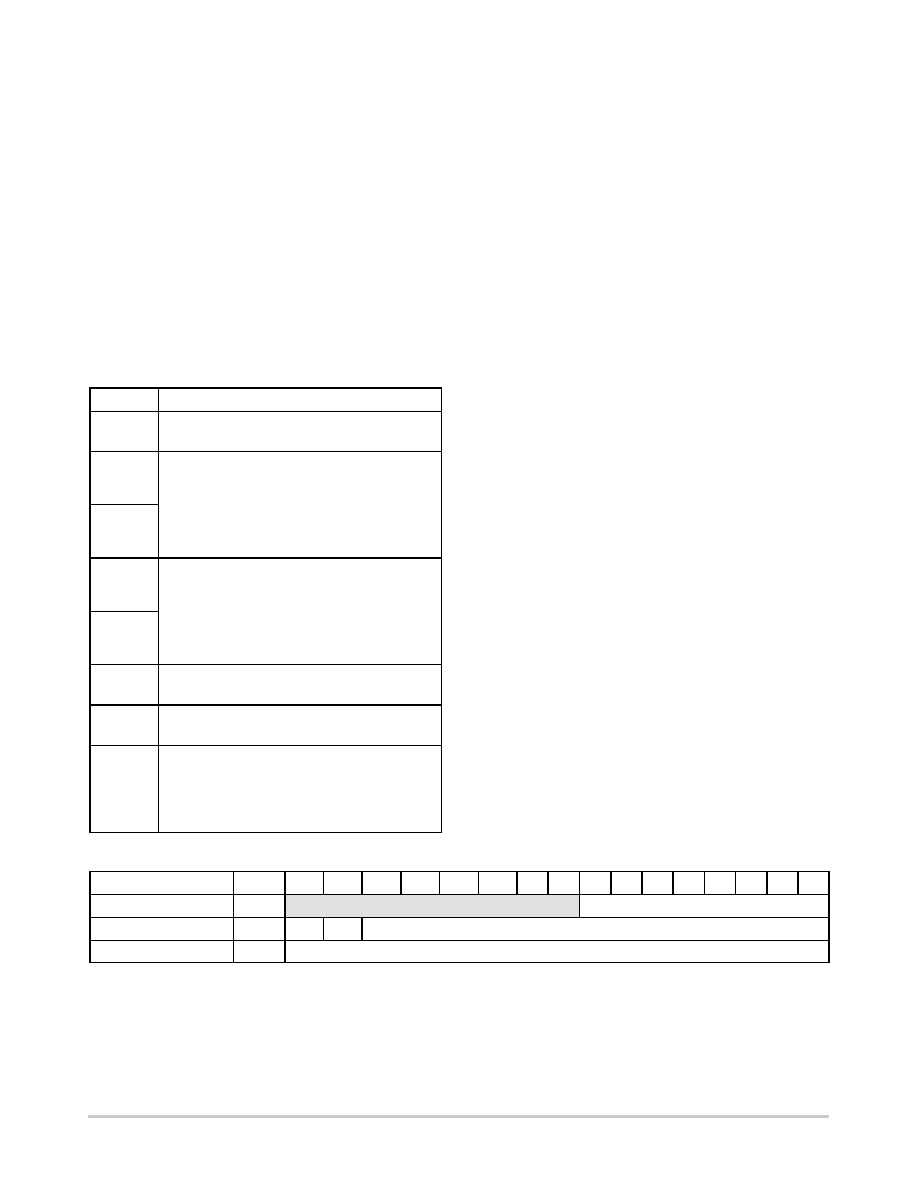
Table 9. INTERNAL REGISTER DESCRIPTION
Bit
Description
0 (LSB)
0 = DAC in 14bit mode
1 = DAC in 16bit mode
1
Set the crystal divide so that CLK2 is 460.8 kHz
Bit 2
Bit 1
0
Crystal/2
0
1
Crystal/4
1
0
Crystal/1
1
Crystal/4
2
3
Set the crystal divide for CLK1
Bit 4
Bit 3
0
Crystal/2
0
1
Crystal/4
1
0
Crystal/1
1
Crystal/4
4
5
0 = Watchdog kick external (pin)
1 = Watchdog kick internal (1.8 kHz)
6
0 = RTZ output format on DAC
1 = Non RTZ output format on DAC
7 (MSB)
0 = RxD is low when carrier is off
1 = RxD is high when carrier is off
Setting this bit, changes the function of RxD to
the function of RxD_ENH
Internal Register
The NCN5192 has an 8 bit register to setup its internal
operation. An 8 bit SPI communication method is used to
write to the mode register. If CS goes low after only 8 clock
cycles of SCLK the Mode register will latch in the 8 bits
which are shifted into the SPI shift register. In Table 9 an
explanation of the usage of each bit is given. All bits are set
to ‘0’ at reset.
Sigma Delta DAC
The NCN5192 Modem has an integrated SigmaDelta
Modulator for use in a current loop slave transmitter.
Through this DAC, an analog value can be set and
transmitted across the current loop. For more information on
how to create a current loop slave transmitter, see
application notes on the ON Semi website. The DAC output
will switch between 0 V and the voltage provided to
DACREF. To achieve maximum accuracy, the DACREF
voltage should be kept stable, so that power supply
variations are not visible in the DAC output. The
SigmaDelta modulator output can be set through SPI
frames containing 14 or 16 significant bits. The length of the
data frames can be set through bit 0 is the status register. The
output of the DAC can be set return to zero (RTZ) or
nonRTZ. This is important when the rise and fall time of the
signal are not identical. This will cause a DC offset
depending on the number of rising and falling edges. As the
output bits of a sigmadelta modulator are randomly
arranged (ie. for the same setting we could get 01110000 or
01010100), the number of edges might vary over time for a
non return to zero signal. Setting the DAC to “return to zero”
forces the output to have a rising and falling edge for each
logic “1” bit, so that no offset from pulse asymmetry can
occur. However, this will decrease the range of the
modulator to 50% of DACREF, as the maximum duty cycle
is 50% instead of 100% for NRZ. When a clock failure is
detected, using an internal oscillator, the DAC output will
jump to the level set by the JUMP pin, until the IC is reset
or a rising flank is detected on KICK.
Table 10. SPI FRAME FORMAT
Description
Bits
15
14
13
12
11
10
9
8
7
6
5
4
3
2
1
0
Mode Register
8
Mode Register Data
DAC – 14 bits mode
16
0
DAC Output Word
DAC – 16 bits mode
16
DAC Output Word
相關(guān)PDF資料 |
PDF描述 |
|---|---|
| NCV1455BDR2 | IC OSC MONO TIMING 8SOIC |
| NMF3010FCT1G | IC LINE FILTER SIGNAL 6FLIPCHIP |
| PCA2002TK/1,118 | IC WATCH CIRCUIT 10HVSON |
| PCKV857EV,118 | IC 1:10 2.5V PLL CLK-DRVR48TSSOP |
| PCM1602APTG4 | IC DAC 24BIT 6CH 192KHZ 48-LQFP |
相關(guān)代理商/技術(shù)參數(shù) |
參數(shù)描述 |
|---|---|
| NCN6000 | 制造商:ONSEMI 制造商全稱:ON Semiconductor 功能描述:Compact Smart Card Interface IC |
| NCN6000/D | 制造商:未知廠家 制造商全稱:未知廠家 功能描述:Compact Smart Card Interface IC |
| NCN6000DTB | 功能描述:輸入/輸出控制器接口集成電路 2.7V POS/ATM Smart RoHS:否 制造商:Silicon Labs 產(chǎn)品: 輸入/輸出端數(shù)量: 工作電源電壓: 最大工作溫度:+ 85 C 最小工作溫度:- 40 C 安裝風(fēng)格:SMD/SMT 封裝 / 箱體:QFN-64 封裝:Tray |
| NCN6000DTBG | 功能描述:輸入/輸出控制器接口集成電路 2.7V POS/ATM Smart Card Interface RoHS:否 制造商:Silicon Labs 產(chǎn)品: 輸入/輸出端數(shù)量: 工作電源電壓: 最大工作溫度:+ 85 C 最小工作溫度:- 40 C 安裝風(fēng)格:SMD/SMT 封裝 / 箱體:QFN-64 封裝:Tray |
| NCN6000DTBR2 | 功能描述:輸入/輸出控制器接口集成電路 2.7V POS/ATM Smart RoHS:否 制造商:Silicon Labs 產(chǎn)品: 輸入/輸出端數(shù)量: 工作電源電壓: 最大工作溫度:+ 85 C 最小工作溫度:- 40 C 安裝風(fēng)格:SMD/SMT 封裝 / 箱體:QFN-64 封裝:Tray |
發(fā)布緊急采購,3分鐘左右您將得到回復(fù)。