- 您現(xiàn)在的位置:買賣IC網(wǎng) > PDF目錄299526 > MX602-020.48M (CONNOR WINFIELD CORP) TCXO, CLOCK, 20.48 MHz, LVCMOS OUTPUT PDF資料下載
參數(shù)資料
| 型號: | MX602-020.48M |
| 廠商: | CONNOR WINFIELD CORP |
| 元件分類: | XO, clock |
| 英文描述: | TCXO, CLOCK, 20.48 MHz, LVCMOS OUTPUT |
| 封裝: | ROHS COMPLIANT, HERMETIC SEALED, CERAMIC PACKAGE-10 |
| 文件頁數(shù): | 2/2頁 |
| 文件大小: | 323K |
| 代理商: | MX602-020.48M |
Specifications subject to change without notice. All dimensions in inches. Copyright 2010 The Connor-Winfield Corporation
2111 Comprehensive Drive
Aurora, Illinois 60505
Phone: 630- 851- 4722
Fax: 630- 851- 5040
www.conwin.com
Bulletin
TX303
Page
2 of 2
Revision
02
Date
21 Oct 2010
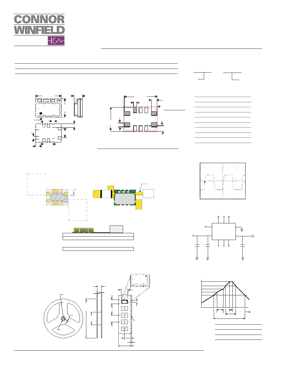
Suggested Pad Layout
Ordering Information
Design Recommendations
Output Waveform
Tape and Reel Dimensions
Environmental Characteristics
Vibration:
Vibration per Mil Std 883E Method 2007.3 Test Condition A
Shock:
Mechanical Shock per Mil Std 883E Method 2002.4 Test Condition B.
Soldering Process;
RoHS compliant lead free. See soldering profile on page 2.
1:
Do Not Connect
2:
Do Not Connect
3:
Do Not Connect
4:
Ground
5:
Output
6:
Do Not Connect
7:
Do Not Connect
8:
Enable /Disable
9:
Supply Voltage Vcc
10:
N/C
Pad Connections
Solder Profile
120°C
150°C
180°C
260°C
0
220°C
360 Sec. Max.
120 S
Max.
10 S
60 S
Max.
Time
Temperature
260°C
120°C
150°C
180°C
260°C
0
220°C
360 Sec. Max.
120 S
Max.
10 S
60 S
Max.
Time
Temperature
260°C
Package Layout
0.276
0.006
(7.0mm)
±
0.197
0.006
(5.0mm)
±
0.079 Max.
(2.0mm)
MX602 1005
12.8 MHz
0.025(6 Places)
(0.635mm)
0.100
(2.54mm)
0.040
(1.02mm)
(6 Places)
0.030
(0.762mm)
(4 Places)
0.100
(2.54mm)
Pin 1
0.038
(0.965mm)
(4 Places)
Dimensional Tolerance:
±.005 (.127mm)
±.02
(.508mm)
1
2
3
4
5
6
7
8
9
10
Bottom
View
MX602
-
020.48M
TCXO
SERIES
CENTER
FREQUENCY
MX602
-
012.8M
MX602
-
010.24M
MEETS EIA-481A and EIAJ-1009B
2,000 PCS/REEL
8.46 DIA
(216mm DIA)
.08
(2.0mm)
1.00 DIA
(25mm DIA)
9.84 DIA
(250mm DIA)
.06 DIA
(1.5mm DIA)
.69
(17.5mm)
.08
(2.0mm)
3.15
(80mm)
.315
(8.0mm)
.08
(2.0mm)
.21
(5.4mm)
.157
(4.0mm)
.31
(7.9mm)
.295 (7.5mm)
.07 (1.75mm)
.83 (16.0mm)
PIN 1
0.215
(5.46mm)
0.037
(0.94mm)
0.051
(1.28mm)
0.051
(1.28mm)
0.295
(7.49mm)
0.030
(0.76mm)
Keep Out Area
Top View
1
10
9
5
4
8
2
3
6
7
* Do not route any traces in the keep out area. It is
recommended the next layer under the keep out area
is to be ground plane.
*
4
5
1
2
3
6
7
8
9
10
Vcc
Supply
Voltage
N/C
DNC
DNC DNC
10 nF
Bypass
Enable/
Disable
Output
15 pF
Ground
0.1 uF
Bypass
DNC = Do Not Connect
OSC
TOP LAYER
GROUND LAYER
BOTTOM LAYER
Output
Buffer
50 Ohm Trace
Without
Vias
.......
Vcc, should have
a large copper
area for reduced
inductance.
Connect a 0.01uF
bypass capacitor
<0.1”(2.54mm)
from the pad.
Ground,
should have
a large copper
area for reduced
inductance.
0.010”(0.254mm)
Recommended
clearance
inductance
for internal
copper flood.
Top View
1
3
4
5
6
8
9
10
Buffer
Ground
50 Ohm trace
<1”by design
Vcc
Ground
Top View
Test Circuit
相關(guān)PDF資料 |
PDF描述 |
|---|---|
| MX602-010.24M | TCXO, CLOCK, 10.24 MHz, LVCMOS OUTPUT |
| MXO45-6I-FREQ2 | CRYSTAL OSCILLATOR, CLOCK, 50.1 MHz - 80 MHz, CMOS/TTL OUTPUT |
| MXO45HST-6I-FREQ3 | CRYSTAL OSCILLATOR, CLOCK, 80.1 MHz - 105.561 MHz, CMOS/TTL OUTPUT |
| MXO45HS-6I-FREQ3 | CRYSTAL OSCILLATOR, CLOCK, 80.1 MHz - 105.561 MHz, CMOS/TTL OUTPUT |
| MXO45HST-6I-FREQ1 | CRYSTAL OSCILLATOR, CLOCK, 1 MHz - 50 MHz, CMOS/TTL OUTPUT |
相關(guān)代理商/技術(shù)參數(shù) |
參數(shù)描述 |
|---|---|
| MX604DW | 制造商:CML Innovative Technologies 功能描述:V.23 Modem, Tube |
| MX604P | 制造商:CML Innovative Technologies 功能描述:V.23 Modem, Tube |
| MX604TN | 制造商:CML Innovative Technologies 功能描述:V.23 Modem, Tube |
| MX609DW | 制造商:CML Innovative Technologies 功能描述:Delta Modulation Codec, Tube |
| MX609LH | 制造商:CML Innovative Technologies 功能描述:Delta Modulation Codec, Tube 制造商:MXCOM 功能描述: |
發(fā)布緊急采購,3分鐘左右您將得到回復(fù)。