- 您現(xiàn)在的位置:買賣IC網(wǎng) > PDF目錄299526 > MX602-020.48M (CONNOR WINFIELD CORP) TCXO, CLOCK, 20.48 MHz, LVCMOS OUTPUT PDF資料下載
參數(shù)資料
| 型號: | MX602-020.48M |
| 廠商: | CONNOR WINFIELD CORP |
| 元件分類: | XO, clock |
| 英文描述: | TCXO, CLOCK, 20.48 MHz, LVCMOS OUTPUT |
| 封裝: | ROHS COMPLIANT, HERMETIC SEALED, CERAMIC PACKAGE-10 |
| 文件頁數(shù): | 1/2頁 |
| 文件大?。?/td> | 323K |
| 代理商: | MX602-020.48M |
Specifications subject to change without notice. All dimensions in inches. Copyright 2010 The Connor-Winfield Corporation
2111 Comprehensive Drive
Aurora, Illinois 60505
Phone: 630- 851- 4722
Fax: 630- 851- 5040
www.conwin.com
2111 Comprehensive Drive
Aurora, Illinois 60505
Phone: 630- 851- 4722
Fax: 630- 851- 5040
www.conwin.com
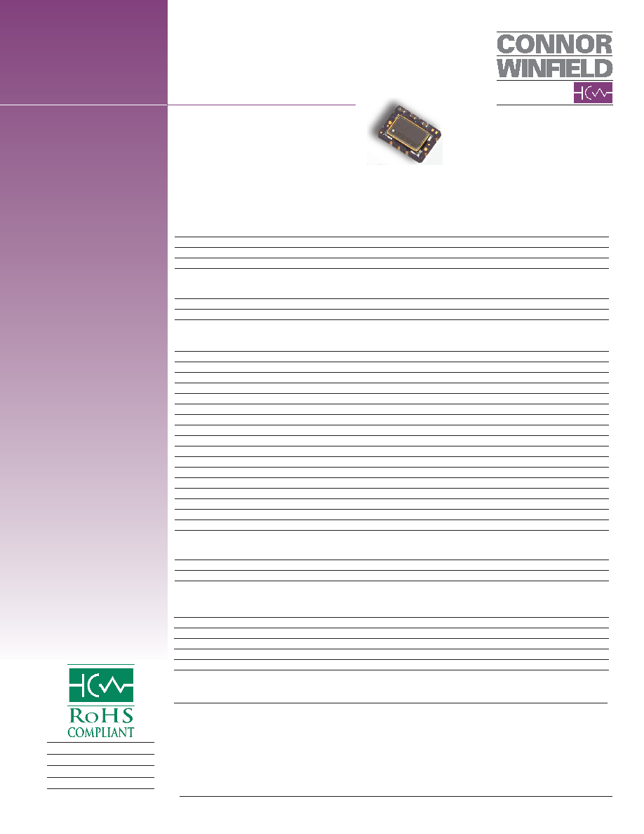
5x7mm Surface Mount
Precision TCXO
Model MX602
Description:
The Connor-Winfield MX602 is a Surface
Mount, 5x7mm, 3.3V, LVCMOS Temperature
Compensated Crystal Oscillators (TCXO)
designed for applications requiring tight
frequency stability. The RoHS compliant surface
mount package is designed for high-density mounting and is
optimum for mass production. The MX602 TCXO has been
approved by Maxim for use with their Timing IC DS310x
series.
Operating Specifications
Parameter
Minimum
Nominal
Maximum
Units
Notes
Nominal Frequency (Fo)
-
10.24, 12.80, or 20.48
-
MHz
Frequency Calibration @ 25 °C
-1.0
-
1.0
ppm
1
Frequency Stability
Frequency Vs. Temperature
-0.28
-
0.28
ppm
2
Holdover Stability (24 Hours)
-0.32
-
0.32
ppm
3
Aging / Day
-40
-
40
ppb
Aging / Life
-3.0
-
3.0
ppm
Aging / Second
-
4.6E-13
-
Frequency vs. Load Stability
-50
-
50
ppb
±5%, 4
Frequency vs. Voltage Stability
-50
-
50
ppb
±5%
Total Frequency Tolerance
-4.6
-
4.6
ppm
5
Operating Temperature Range:
-40
-
85
°C
Supply Voltage (Vcc)
3.135
3.3
3.465
Vdc
±5%
Supply Current (Icc)
-
6
10
mA
Period Jitter
-
3
5
ps rms
Integrated Phase Jitter
-
0.3
1.0
ps rms
SSB Phase Noise at 10Hz offset
-
-90
-85
dBc/Hz
SSB Phase Noise at 100Hz offset
-
-120
-115
dBc/Hz
SSB Phase Noise at 1KHz offset
-
-140
-135
dBc/Hz
SSB Phase Noise at 10KHz offset
-
-150
-145
dBc/Hz
SSB Phase Noise at 100KHz offset
-
-152
-150
dBc/Hz
Start-up Time
-
1
ms
Absolute Maximum Ratings
Parameter
Minimum
Nominal
Maximum
Units
Notes
Storage Temperature
-40
-
85
°C
Supply Voltage (Vcc)
-0.5
-
6.0
Vdc
Input Voltage
-0.5
-
Vcc+0.6
Vdc
Features:
Model: MX602
3.3 Vdc Operation
Frequency Stability: ± 0.28 ppm
Temperature Range: -40 to 85°C
LVCMOS Output
Ceramic Surface Mount Package
Tape and Reel Packaging
RoHS Compliant / Pb Free
Bulletin
TX303
Page
1 of 2
Revision
02
Date
21 Oct 2010
US Headquarters:
630-851-4722
European Headquarters:
+353-61-472221
LVCMOS Output Characteristics
Parameter
Minimum
Nominal
Maximum
Units
Notes
Load
-
15
-
pF
7
Voltage (High)
(Voh)
90%Vcc
-
Vdc
(Low)
(Vol)
-
10%Vcc
Vdc
Duty Cycle at 50% of Vcc
45
50
55
%
Rise / Fall Time 10% to 90%
-
4
8
ns
Package Characteristics
Package
Hermetically sealed ceramic package and metal cover
MX602
1005
12.
8
M
Hz
Notes:
1. Frequency referenced to Fo.
2. Frequency stability vs. change in temperature. [±(Fmax - Fmin)/2.Fo].
3. Inclusive of frequency stability vs. change in temperature , supply voltage change and aging over a 24 hour period.
4. Referenced to 15 pF.
5. Inclusive of calibration@25°C, frequency vs. change in temperature, change in supply voltage(±5%), load change(±5%) and 20 years aging.
6. Output is enabled with no connection on pad 8.
7 Attention: To achieve optimal frequency stability, and in some cases to meet the specification stated on this data sheet, it is required that the
circuit connected to this TCXO output must have the equivalent input capacitance that is specified by the nominal load capacitance. Deviations
from the nominal load capacitance will have a graduated effect on the stability of approximately 20 ppb per pF load difference.
Enable / Disable Input Characteristics
Parameter
Minimum
Nominal
Maximum
Units
Notes
Enable Voltage (High)
70%Vcc
-
Vdc
6
Disable Voltage (Low)
-
30%Vcc
Vdc
相關(guān)PDF資料 |
PDF描述 |
|---|---|
| MX602-010.24M | TCXO, CLOCK, 10.24 MHz, LVCMOS OUTPUT |
| MXO45-6I-FREQ2 | CRYSTAL OSCILLATOR, CLOCK, 50.1 MHz - 80 MHz, CMOS/TTL OUTPUT |
| MXO45HST-6I-FREQ3 | CRYSTAL OSCILLATOR, CLOCK, 80.1 MHz - 105.561 MHz, CMOS/TTL OUTPUT |
| MXO45HS-6I-FREQ3 | CRYSTAL OSCILLATOR, CLOCK, 80.1 MHz - 105.561 MHz, CMOS/TTL OUTPUT |
| MXO45HST-6I-FREQ1 | CRYSTAL OSCILLATOR, CLOCK, 1 MHz - 50 MHz, CMOS/TTL OUTPUT |
相關(guān)代理商/技術(shù)參數(shù) |
參數(shù)描述 |
|---|---|
| MX604DW | 制造商:CML Innovative Technologies 功能描述:V.23 Modem, Tube |
| MX604P | 制造商:CML Innovative Technologies 功能描述:V.23 Modem, Tube |
| MX604TN | 制造商:CML Innovative Technologies 功能描述:V.23 Modem, Tube |
| MX609DW | 制造商:CML Innovative Technologies 功能描述:Delta Modulation Codec, Tube |
| MX609LH | 制造商:CML Innovative Technologies 功能描述:Delta Modulation Codec, Tube 制造商:MXCOM 功能描述: |
發(fā)布緊急采購,3分鐘左右您將得到回復(fù)。