- 您現(xiàn)在的位置:買賣IC網(wǎng) > PDF目錄371153 > MTP8N06E (MOTOROLA INC) TMOS POWER FET 8.0 AMPERES 60 VOLTS RDS(on) = 0.12 OHM PDF資料下載
參數(shù)資料
| 型號: | MTP8N06E |
| 廠商: | MOTOROLA INC |
| 元件分類: | JFETs |
| 英文描述: | TMOS POWER FET 8.0 AMPERES 60 VOLTS RDS(on) = 0.12 OHM |
| 中文描述: | 8 A, 60 V, 0.12 ohm, N-CHANNEL, Si, POWER, MOSFET, TO-220AB |
| 文件頁數(shù): | 2/8頁 |
| 文件大?。?/td> | 212K |
| 代理商: | MTP8N06E |
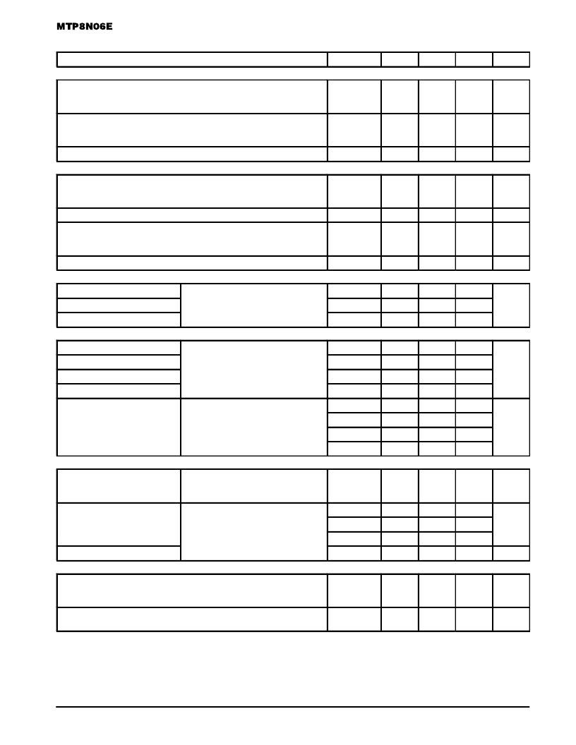
2
Motorola TMOS Power MOSFET Transistor Device Data
ELECTRICAL CHARACTERISTICS
(TJ = 25
°
C unless otherwise noted)
Characteristic
Symbol
Min
Typ
Max
Unit
OFF CHARACTERISTICS
Drain–Source Breakdown Voltage
(VGS = 0 Vdc, ID = 250
μ
Adc)
Temperature Coefficient (Positive)
V(BR)DSS
60
—
—
63
—
—
Vdc
mV/
°
C
Zero Gate Voltage Drain Current
(VDS = 60 Vdc, VGS = 0 Vdc)
(VDS = 60 Vdc, VGS = 0 Vdc, TJ = 125
°
C)
Gate–Body Leakage Current (VGS =
±
20 Vdc, VDS = 0)
IDSS
—
—
—
—
10
100
μ
Adc
IGSS
—
—
100
nAdc
ON CHARACTERISTICS (1)
Gate Threshold Voltage
(VDS = VGS, ID = 250
μ
Adc)
Temperature Coefficient (Negative)
VGS(th)
2.0
—
3.0
5.0
4.0
—
Vdc
mV/
°
C
Static Drain–Source On–Resistance (VGS = 10 Vdc, ID = 4.0 Adc)
Drain–Source On–Voltage (VGS = 10 Vdc)
(ID = 8.0 Adc)
(ID = 4.0 Adc, TJ = 125
°
C)
RDS(on)
VDS(on)
—
0.087
0.12
Ohm
—
—
0.7
—
1.2
1.0
Vdc
Forward Transconductance (VDS = 10 Vdc, ID = 4.0 Adc)
gFS
3.0
4.8
—
mhos
DYNAMIC CHARACTERISTICS
Input Capacitance
f = 1.0 MHz)
Ciss
Coss
Crss
—
424
570
pF
Output Capacitance
(VDS = 25 Vdc, VGS = 0 Vdc,
—
180
250
Reverse Transfer Capacitance
—
45
90
SWITCHING CHARACTERISTICS (2)
Turn–On Delay Time
RG = 9.1
)
td(on)
tr
td(off)
tf
—
8.0
20
ns
Rise Time
(VDD = 30 Vdc, ID = 8.0 Adc,
VGS = 10 Vdc,
—
31
60
Turn–Off Delay Time
—
21
40
Fall Time
—
25
50
Gate Charge
(See Figure 8)
VGS = 10 Vdc)
QT
Q1
Q2
Q3
—
13.9
20
nC
(VDS = 48 Vdc, ID = 8.0 Adc,
—
2.6
—
—
6.6
—
—
6.1
—
SOURCE–DRAIN DIODE CHARACTERISTICS
Forward On–Voltage (1)
(IS = 8.0 Adc, VGS = 0 Vdc)
(IS = 8.0 Adc, VGS = 0 Vdc, TJ = 125
°
C)
VSD
—
—
0.96
0.85
2.0
—
Vdc
Reverse Recovery Time
(See Figure 14)
dIS/dt = 100 A/
μ
s)
trr
ta
—
59.7
—
ns
(IS = 8.0 Adc, VGS = 0 Vdc,
—
41
—
tb
—
18.7
—
Reverse Recovery Stored Charge
QRR
—
0.142
—
μ
C
INTERNAL PACKAGE INDUCTANCE
Internal Drain Inductance
(Measured from contact screw on tab to center of die)
(Measured from the drain lead 0.25
″
from package to center of die)
LD
—
—
3.5
4.5
—
—
nH
Internal Source Inductance
(Measured from the source lead 0.25
″
from package to source bond pad)
LS
—
7.5
—
nH
(1) Pulse Test: Pulse Width
≤
300
μ
s, Duty Cycle
≤
2%.
(2) Switching characteristics are independent of operating junction temperature.
相關PDF資料 |
PDF描述 |
|---|---|
| MTS102 | Silicon Temperature Sensors |
| MTS103 | Silicon Temperature Sensors |
| MTS105 | Silicon Temperature Sensors |
| MTSF3N02HD | SINGLE TMOS POWER MOSFET 4.0 AMPERES 20 VOLTS RDS(on) = 0.040 OHM |
| MTSF3N03HD | SINGLE TMOS POWER MOSFET 3.8 AMPERES 30 VOLTS RDS(on) = 0.040 OHM |
相關代理商/技術參數(shù) |
參數(shù)描述 |
|---|---|
| MTP8N50E | 制造商:Rochester Electronics LLC 功能描述:- Bulk 制造商:ON Semiconductor 功能描述: |
| MTP8P08 | 制造商:MOTOROLA 制造商全稱:Motorola, Inc 功能描述:POWER FIELD EFFECT TRANSISTOR |
| MTP8P10 | 制造商:MOTOROLA 制造商全稱:Motorola, Inc 功能描述:POWER FIELD EFFECT TRANSISTOR |
| MTP9435BDYQ8 | 制造商:CYSTEKEC 制造商全稱:Cystech Electonics Corp. 功能描述:P-CHANNEL ENHANCEMENT MODE POWER MOSFET |
| MTP9435Q8 | 制造商:CYSTEKEC 制造商全稱:Cystech Electonics Corp. 功能描述:P-CHANNEL ENHANCEMENT MODE POWER MOSFET |
發(fā)布緊急采購,3分鐘左右您將得到回復。