- 您現(xiàn)在的位置:買賣IC網(wǎng) > PDF目錄359235 > MT93L00A (Zarlink Semiconductor Inc.) Multi-Channel Voice Echo Canceller PDF資料下載
參數(shù)資料
| 型號(hào): | MT93L00A |
| 廠商: | Zarlink Semiconductor Inc. |
| 英文描述: | Multi-Channel Voice Echo Canceller |
| 中文描述: | 多通道語(yǔ)音回聲消除器 |
| 文件頁(yè)數(shù): | 6/39頁(yè) |
| 文件大?。?/td> | 636K |
| 代理商: | MT93L00A |
第1頁(yè)第2頁(yè)第3頁(yè)第4頁(yè)第5頁(yè)當(dāng)前第6頁(yè)第7頁(yè)第8頁(yè)第9頁(yè)第10頁(yè)第11頁(yè)第12頁(yè)第13頁(yè)第14頁(yè)第15頁(yè)第16頁(yè)第17頁(yè)第18頁(yè)第19頁(yè)第20頁(yè)第21頁(yè)第22頁(yè)第23頁(yè)第24頁(yè)第25頁(yè)第26頁(yè)第27頁(yè)第28頁(yè)第29頁(yè)第30頁(yè)第31頁(yè)第32頁(yè)第33頁(yè)第34頁(yè)第35頁(yè)第36頁(yè)第37頁(yè)第38頁(yè)第39頁(yè)
MT93L00A
Data Sheet
6
Zarlink Semiconductor Inc.
Device Overview
The MT93L00 architecture contains 32 echo cancellers divided into 16 groups. Each group has two echo
cancellers, Echo Canceller A and Echo Canceller B. Each group can be configured in Normal, Extended Delay or
Back-to-Back configurations. In
Normal configuration
, a group of echo cancellers provides two channels of 64 ms
echo cancellation, which run independently on different channels. In
Extended Delay
configuration, a group of
echo cancellers achieves 128 ms of echo cancellation by cascading the two echo cancellers (A & B). In
Back-to-
Back
configuration, the two echo cancellers from the same group are positioned to cancel echo coming from both
directions in a single channel, providing full-duplex 64 ms echo cancellation.
Each echo canceller contains the following main elements (see Figure 4).
Adaptive Filter for estimating the echo channel
Subtractor for cancelling the echo
Double-Talk detector for disabling the filter adaptation during periods of double-talk
Path Change detector for fast reconvergence on major echo path changes
Instability Detector to combat oscillation in very low ERL environments
Non-Linear Processor for suppression of residual echo
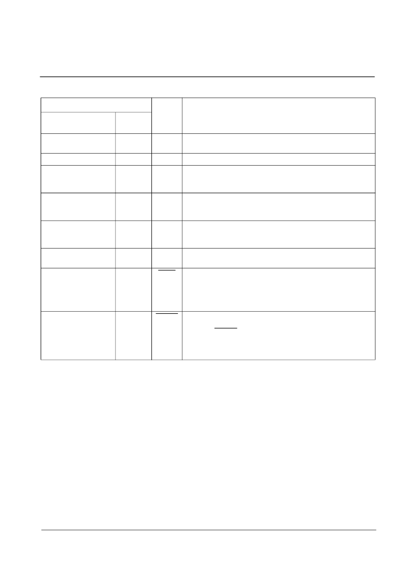
K3
95,97
PLLVss1
PLLVss2
PLL Ground.
Must be connected to V
SS.
K4
96
PLLV
DD
PLL Power Supply.
Must be connected to V
DD2.
TMS
Test Mode Select (3.3 V Input).
JTAG signal that controls the
state transitions of the TAP controller. This pin is pulled high by
an internal pull-up when not driven.
M2
1
M1
2
TDI
Test Serial Data In (3.3 V Input).
JTAG serial test instructions
and data are shifted in on this pin. This pin is pulled high by an
internal pull-up when not driven.
N1
3
TDO
Test Serial Data Out (Output).
JTAG serial data is output on this
pin on the falling edge of TCK. This pin is held in high impedance
state when JTAG scan is not enabled.
P1
4
TCK
Test Clock (3.3 V Input).
Provides the clock to the JTAG test
logic.
N2
6
TRST
Test Reset (3.3 V Input).
Asynchronously initializes the JTAG
TAP controller by putting it in the Test-Logic-Reset state. This pin
should be pulsed low on power-up or held low, to ensure that the
MT93L00 is in the normal functional mode. This pin is pulled by
an internal pull-down when not driven.
R3
8
RESET
Device Reset (Schmitt Trigger Input).
An active low resets the
device and puts the MT93L00 into a low-power stand-by mode.
When the RESET pin is returned to logic high and a clock is
applied to the MCLK pin, the device will automatically execute
initialization routines, which preset all the Control and Status
Registers to their default power-up values.
Pin Description (continued)
PIN #
PIN
Name
Description
208-Ball LBGA
100 PIN
LQFP
相關(guān)PDF資料 |
PDF描述 |
|---|---|
| MT93L04 | 128-Channel Voice Echo Canceller |
| MT9LD272G-6S | x72 Fast Page Mode DRAM Module |
| MT9LD272G-6XS | x72 EDO Page Mode DRAM Module |
| MT9LD272G-7S | x72 Fast Page Mode DRAM Module |
| MT9LD272G-7XS | x72 EDO Page Mode DRAM Module |
相關(guān)代理商/技術(shù)參數(shù) |
參數(shù)描述 |
|---|---|
| MT93L00AB | 制造商:Microsemi Corporation 功能描述:ECHO CANCELLER CHIP 32CH G.164/G.165/G.168/G.711 W/ TONE DET - Trays |
| MT93L00AV | 制造商:Microsemi Corporation 功能描述:ECHO CANCELLER CHIP 32CH G.164/G.165/G.168/G.711 W/ TONE DET - Trays 制造商:MICROSEMI CONSUMER MEDICAL PRODUCT GROUP 功能描述:IC VOICE ECHO CANCELLER 208PBGA 制造商:Microsemi Corporation 功能描述:IC VOICE ECHO CANCELLER 208PBGA |
| MT93L04 | 制造商:ZARLINK 制造商全稱:Zarlink Semiconductor Inc 功能描述:128-Channel Voice Echo Canceller |
| MT93L04A | 制造商:ZARLINK 制造商全稱:Zarlink Semiconductor Inc 功能描述:128-Channel Voice Echo Canceller |
| MT93L04AG | 制造商:Microsemi Corporation 功能描述:ECHO CANCELLER CHIP 128CH G.164/G.165/G.168/G.711 W/ TONE DE - Trays 制造商:MICROSEMI CONSUMER MEDICAL PRODUCT GROUP 功能描述:IC VOICE ECHO CANCEL 365MCMBGA |
發(fā)布緊急采購(gòu),3分鐘左右您將得到回復(fù)。