- 您現(xiàn)在的位置:買賣IC網(wǎng) > PDF目錄383642 > MT88L85 (Mitel Networks Corporation) 3V Integrated DTMFTransceiver with Power Down & Adaptive Micro Interface PDF資料下載
參數(shù)資料
| 型號: | MT88L85 |
| 廠商: | Mitel Networks Corporation |
| 英文描述: | 3V Integrated DTMFTransceiver with Power Down & Adaptive Micro Interface |
| 中文描述: | 3V的集成DTMFTransceiver與掉電 |
| 文件頁數(shù): | 9/20頁 |
| 文件大小: | 350K |
| 代理商: | MT88L85 |
Advance Information
MT88L85
4-79
(DS). When DS is low,
Motorola processor operation
is selected.
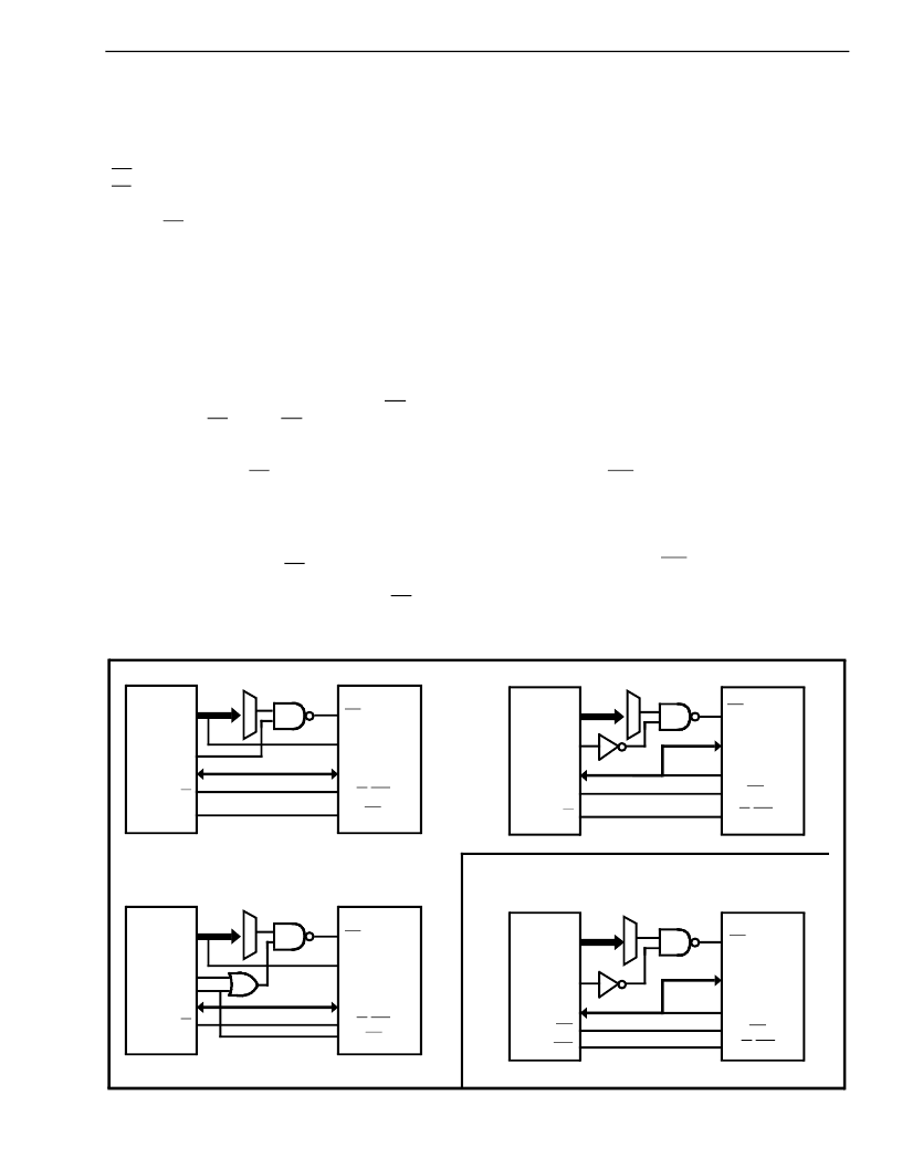
Figure 17 shows the timing diagram for the Motorola
MC68HC11 (1 MHz) microcontroller. The chip select
(CS) input is formed by NANDing address strobe
(AS) and address decode output. Again, the
MT88L85 examines the state of DS on the falling
edge of CS to determine if the micro has a Motorola
bus (when DS is low). Additionally, the Texas
Instruments TMS370CX5X is qualified to have a
Motorola
interface.
Figure
connection of these Motorola processors to the
MT88L85 DTMF transceiver.
12(a)
summarizes
Figures 18 and 19 are the timing diagrams for the
Intel 8031/8051 (12 MHz) and 8085 (5 MHz) micro-
controllers with multiplexed address and data buses.
The MT88L85 latches in the state of RD on the
falling edge of CS. When RD is high, Intel processor
operation is selected. By NANDing the address
latch enable (ALE) output with the high-byte address
(P2) decode output, CS can be generated. Figure
12(b) summarizes the connection of these Intel
processors to the MT88L85 transceiver.
NOTE:
The adaptive micro interface relies on high-
to-low
transition
on
microcontroller interface and this pin must not be tied
permanently low.
CS
to
recognize
the
The adaptive micro interface provides access to five
internal registers. The read-only Receive Data
Register contains the decoded output of the last
valid DTMF digit received. Data entered into the
write-only Transmit Data Register will determine
which tone pair is to be generated (see Table 1 for
coding details). Transceiver control is accomplished
with two control registers (see Tables 6 and 7), CRA
and CRB, which have the same address. A write
operation to CRB is executed by first setting the
most significant bit (b3) in CRA. The following write
operation to the same address will then be directed
to CRB, and subsequent write cycles will be directed
back to CRA. The read-only status register indicates
the current transceiver state (see Table 8).
A software reset must be included at the beginning
of all programs to initialize the control registers upon
power-up or power reset (see Figure 14). Refer to
Tables 4-7 for bit descriptions of the two control
registers.
The multiplexed IRQ/CP pin can be programmed to
generate an interrupt upon validation of DTMF
signals or when the transmitter is ready for more
data (burst mode only). Alternatively, this pin can be
configured to provide a square-wave output of the
call progress signal. The IRQ/CP pin is an open drain
output and requires an external pull-up resistor (see
Figure 13).
Figure 12 a) & b) - MT88L85 Interface Connections for Various Intel and Motorola Micros
MC6800/6802
MT88L85
MT88L85
A0-A15
VMA
D0-D3
RW
Φ
2
MC68HC11
MC6809
MT88L85
MT88L85
8031/8051
8080/8085
CS
RS0
D0-D3
R/W/WR
DS/RD
A8-A15
AS
AD0-AD3
RW
CS
RS0
DS/RD
D0-D3
R/W/WR
DS
A0-A15
Q
E
D0-D3
R/W
CS
RS0
D0-D3
R/W/WR
DS/RD
A8-A15
ALE
P0
RD
WR
CS
D0-D3
RS0
DS/RD
R/W/WR
(a)
(b)
相關(guān)PDF資料 |
PDF描述 |
|---|---|
| MT88L85AE | 3V Integrated DTMFTransceiver with Power Down & Adaptive Micro Interface |
| MT88L85AN | 3V Integrated DTMFTransceiver with Power Down & Adaptive Micro Interface |
| MT88L85AP | 3V Integrated DTMFTransceiver with Power Down & Adaptive Micro Interface |
| MT88L89 | 3V Integrated DTMFTransceiver with Adaptive Micro Interface |
| MT88L89AC | 3V Integrated DTMFTransceiver with Adaptive Micro Interface |
相關(guān)代理商/技術(shù)參數(shù) |
參數(shù)描述 |
|---|---|
| MT88L85AE | 制造商:MITEL 制造商全稱:Mitel Networks Corporation 功能描述:3V Integrated DTMFTransceiver with Power Down & Adaptive Micro Interface |
| MT88L85AE1 | 制造商:Microsemi Corporation 功能描述:DTMF TXRX 3.58MHZ CMOS 3V 24PDIP - Rail/Tube 制造商:MICROSEMI CONSUMER MEDICAL PRODUCT GROUP 功能描述:IC TXRX DTMF 3V 24PDIP 制造商:Microsemi Corporation 功能描述:IC TXRX DTMF 3V 24PDIP |
| MT88L85AN | 制造商:Microsemi Corporation 功能描述: |
| MT88L85AN1 | 制造商:Microsemi Corporation 功能描述:DTMF TXRX 3.58MHZ CMOS 3V 24SSOP - Rail/Tube 制造商:Microsemi Corporation 功能描述:3V DTMF TRANSCEIVER |
| MT88L85ANR | 制造商:Microsemi Corporation 功能描述: |
發(fā)布緊急采購,3分鐘左右您將得到回復(fù)。