- 您現(xiàn)在的位置:買賣IC網(wǎng) > PDF目錄296642 > MT48V4M32TG-8XT 4M X 32 SYNCHRONOUS DRAM, 7 ns, PDSO54 PDF資料下載
參數(shù)資料
| 型號: | MT48V4M32TG-8XT |
| 元件分類: | DRAM |
| 英文描述: | 4M X 32 SYNCHRONOUS DRAM, 7 ns, PDSO54 |
| 封裝: | 0.400 INCH, PLASTIC, TSOP2-54 |
| 文件頁數(shù): | 13/69頁 |
| 文件大?。?/td> | 6213K |
| 代理商: | MT48V4M32TG-8XT |
第1頁第2頁第3頁第4頁第5頁第6頁第7頁第8頁第9頁第10頁第11頁第12頁當前第13頁第14頁第15頁第16頁第17頁第18頁第19頁第20頁第21頁第22頁第23頁第24頁第25頁第26頁第27頁第28頁第29頁第30頁第31頁第32頁第33頁第34頁第35頁第36頁第37頁第38頁第39頁第40頁第41頁第42頁第43頁第44頁第45頁第46頁第47頁第48頁第49頁第50頁第51頁第52頁第53頁第54頁第55頁第56頁第57頁第58頁第59頁第60頁第61頁第62頁第63頁第64頁第65頁第66頁第67頁第68頁第69頁
128Mb: x16, x32
MOBILE SDRAM
09005aef8071a76b
Micron Technology, Inc., reserves the right to change products or specifications without notice.
128Mbx16x32Mobile_2.fm - Rev. G (DRAFT) 7/04 EN
20
2001 Micron Technology, Inc. All rights reserved.
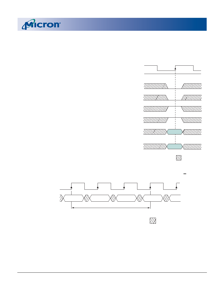
Operation
BANK/ROW ACTIVATION
Before any READ or WRITE commands can be
issued to a bank within the SDRAM, a row in that bank
must be “opened.” This is accomplished via the
ACTIVE command, which selects both the bank and
the row to be activated (seeFigure 10).
After opening a row (issuing an ACTIVE command),
a READ or WRITE command may be issued to that row,
subject to the tRCD specification. tRCD (MIN) should
be divided by the clock period and rounded up to the
next whole number to determine the earliest clock
edge after the ACTIVE command on which a READ or
WRITE command can be entered. For example, a tRCD
specification of 20ns with a 125 MHz clock (8ns
period) results in 2.5 clocks, rounded to 3. This is
reflected in Figure 11, which covers any case where 2 <
tRCD (MIN)/tCK
≤ 3. (The same procedure is used to
convert other specification limits from time units to
clock cycles.)
A subsequent ACTIVE command to a different row
in the same bank can only be issued after the previous
active row has been “closed” (precharged). The mini-
mum time interval between successive ACTIVE com-
mands to the same bank is defined by tRC.
A subsequent ACTIVE command to another bank
can be issued while the first bank is being accessed,
which results in a reduction of total row-access over-
head. The minimum time interval between successive
ACTIVE commands to different banks is defined by
tRRD.
Figure 10: Activating a Specific Row in
a Specific Bank
Figure 11: Example: Meeting tRCD (MIN) When 2 < tRCD (MIN)/tCK< 3
CS#
WE#
CAS#
RAS#
CKE
CLK
A0–A10, A11
ROW
ADDRESS
DON’T CARE
HIGH
BA0, BA1
BANK
ADDRESS
CLK
T2
T1
T3
T0
t
COMMAND
NOP
ACTIVE
READ or
WRITE
T4
NOP
RCD
DON’T CARE
相關(guān)PDF資料 |
PDF描述 |
|---|---|
| MT48LC8M8A2TG-8EL:GIT | 8M X 8 SYNCHRONOUS DRAM, 6 ns, PDSO54 |
| MT4JSF6464HIY-80BXX | 64M X 64 DDR DRAM MODULE, ZMA204 |
| MT4JSF6464HY-1G4XX | 64M X 64 DDR DRAM MODULE, ZMA204 |
| MT4LC16M4A7DJ-6S | 16M X 4 FAST PAGE DRAM, 60 ns, PDSO32 |
| MT58L128L36P1T-5 | 128K X 36 CACHE SRAM, 2.8 ns, PQFP100 |
相關(guān)代理商/技術(shù)參數(shù) |
參數(shù)描述 |
|---|
發(fā)布緊急采購,3分鐘左右您將得到回復。