- 您現(xiàn)在的位置:買賣IC網(wǎng) > PDF目錄384756 > MT48LC8M16A2FC-7E (Micron Technology, Inc.) SYNCHRONOUS DRAM PDF資料下載
參數(shù)資料
| 型號: | MT48LC8M16A2FC-7E |
| 廠商: | Micron Technology, Inc. |
| 英文描述: | SYNCHRONOUS DRAM |
| 中文描述: | 同步DRAM |
| 文件頁數(shù): | 15/59頁 |
| 文件大小: | 1822K |
| 代理商: | MT48LC8M16A2FC-7E |
第1頁第2頁第3頁第4頁第5頁第6頁第7頁第8頁第9頁第10頁第11頁第12頁第13頁第14頁當前第15頁第16頁第17頁第18頁第19頁第20頁第21頁第22頁第23頁第24頁第25頁第26頁第27頁第28頁第29頁第30頁第31頁第32頁第33頁第34頁第35頁第36頁第37頁第38頁第39頁第40頁第41頁第42頁第43頁第44頁第45頁第46頁第47頁第48頁第49頁第50頁第51頁第52頁第53頁第54頁第55頁第56頁第57頁第58頁第59頁
15
128Mb: x4, x8, x16 SDRAM
128MSDRAM_E.p65
–
Rev. E; Pub. 1/02
Micron Technology, Inc., reserves the right to change products or specifications without notice.
2001, Micron Technology, Inc.
128Mb: x4, x8, x16
SDRAM
Operation
BANK/ROW ACTIVATION
Before any READ or WRITE commands can be issued
to a bank within the SDRAM, a row in that bank must be
“opened.” This is accomplished via the ACTIVE com-
mand, which selects both the bank and the row to be
activated (see Figure 3).
After opening a row (issuing an ACTIVE command), a
READ or WRITE command may be issued to that row,
subject to the
t
RCD specification.
t
RCD (MIN) should be
divided by the clock period and rounded up to the next
whole number to determine the earliest clock edge after
the ACTIVE command on which a READ or WRITE com-
mand can be entered. For example, a
t
RCD specification
of 20ns with a 125 MHz clock (8ns period) results in 2.5
clocks, rounded to 3. This is reflected in Figure 4, which
covers any case where 2 <
t
RCD (MIN)/
t
CK
≤
3. (The same
procedure is used to convert other specification limits
from time units to clock cycles.)
A subsequent ACTIVE command to a different row in
the same bank can only be issued after the previous
active row has been “closed” (precharged). The mini-
mum time interval between successive ACTIVE com-
mands to the same bank is defined by
t
RC.
A subsequent ACTIVE command to another bank can
be issued while the first bank is being accessed, which
results in a reduction of total row-access overhead. The
minimum time interval between successive ACTIVE com-
mands to different banks is defined by
t
RRD.
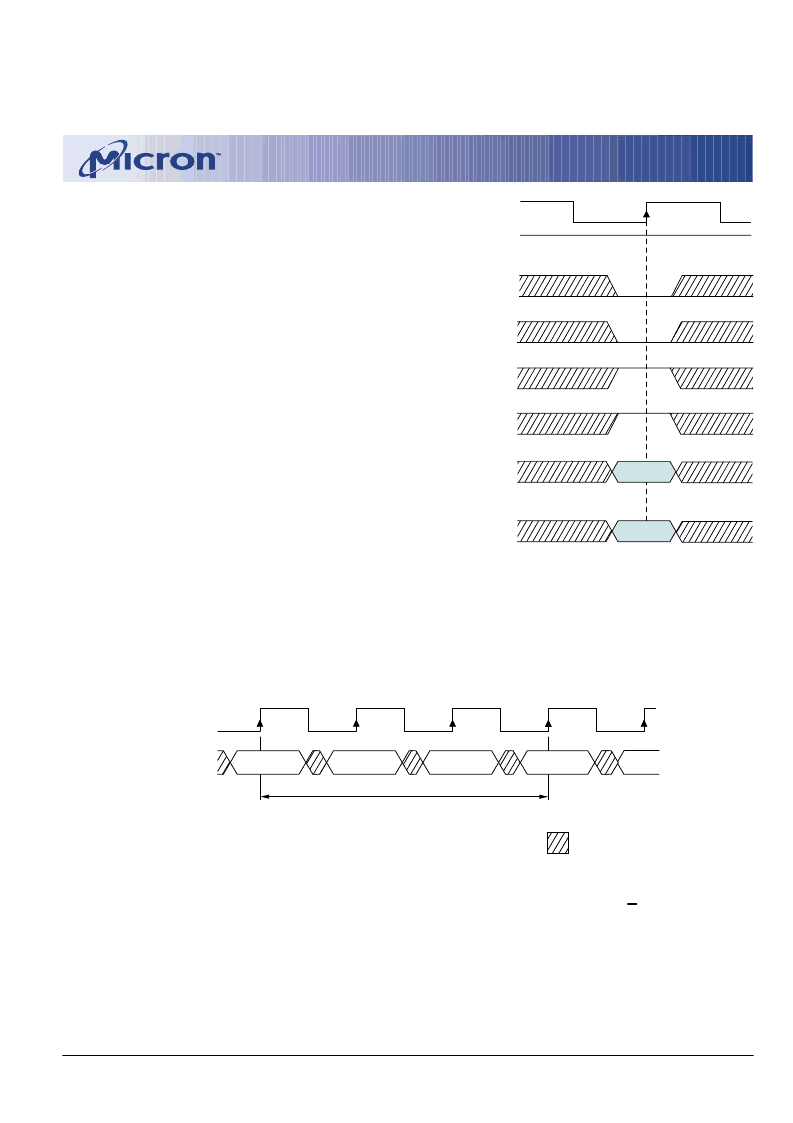
Figure 4
Example: Meeting
t
RCD (MIN) When 2 <
t
RCD (MIN)/
t
CK < 3
CLK
T2
T1
T3
T0
t
COMMAND
NOP
ACTIVE
READ or
WRITE
T4
NOP
RCD
DON
’
T CARE
CS#
WE#
CAS#
RAS#
CKE
CLK
A0
–
A10, A11
ROW
ADDRESS
HIGH
BA0, BA1
BANK
ADDRESS
Figure 3
Activating a Specific Row in a
Specific Bank
相關(guān)PDF資料 |
PDF描述 |
|---|---|
| MT48LC8M16A2FC-7EIT | SYNCHRONOUS DRAM |
| MT48LC8M16A2FC-7EL | SYNCHRONOUS DRAM |
| MT48LC8M16A2FC-7ELIT | SYNCHRONOUS DRAM |
| MT48LC8M16A2FC-8E | SYNCHRONOUS DRAM |
| MT48LC8M16A2FC-8EIT | SYNCHRONOUS DRAM |
相關(guān)代理商/技術(shù)參數(shù) |
參數(shù)描述 |
|---|---|
| MT48LC8M16A2FC-7EIT | 制造商:MICRON 制造商全稱:Micron Technology 功能描述:SYNCHRONOUS DRAM |
| MT48LC8M16A2FC-7EL | 制造商:MICRON 制造商全稱:Micron Technology 功能描述:SYNCHRONOUS DRAM |
| MT48LC8M16A2FC-7ELIT | 制造商:MICRON 制造商全稱:Micron Technology 功能描述:SYNCHRONOUS DRAM |
| MT48LC8M16A2FC-8E | 制造商:MICRON 制造商全稱:Micron Technology 功能描述:SYNCHRONOUS DRAM |
| MT48LC8M16A2FC-8EIT | 制造商:MICRON 制造商全稱:Micron Technology 功能描述:SYNCHRONOUS DRAM |
發(fā)布緊急采購,3分鐘左右您將得到回復。