- 您現(xiàn)在的位置:買賣IC網(wǎng) > PDF目錄384756 > MT48LC8M16A2FC-7E (Micron Technology, Inc.) SYNCHRONOUS DRAM PDF資料下載
參數(shù)資料
| 型號(hào): | MT48LC8M16A2FC-7E |
| 廠商: | Micron Technology, Inc. |
| 英文描述: | SYNCHRONOUS DRAM |
| 中文描述: | 同步DRAM |
| 文件頁數(shù): | 1/59頁 |
| 文件大小: | 1822K |
| 代理商: | MT48LC8M16A2FC-7E |
當(dāng)前第1頁第2頁第3頁第4頁第5頁第6頁第7頁第8頁第9頁第10頁第11頁第12頁第13頁第14頁第15頁第16頁第17頁第18頁第19頁第20頁第21頁第22頁第23頁第24頁第25頁第26頁第27頁第28頁第29頁第30頁第31頁第32頁第33頁第34頁第35頁第36頁第37頁第38頁第39頁第40頁第41頁第42頁第43頁第44頁第45頁第46頁第47頁第48頁第49頁第50頁第51頁第52頁第53頁第54頁第55頁第56頁第57頁第58頁第59頁
1
128Mb: x4, x8, x16 SDRAM
128MSDRAM_E.p65 – Rev. E; Pub. 1/02
Micron Technology, Inc., reserves the right to change products or specifications without notice.
2001, Micron Technology, Inc.
128Mb: x4, x8, x16
SDRAM
PRODUCTS AND SPECIFICATIONS DISCUSSED HEREIN ARE SUBJECT TO CHANGE BY MICRON WITHOUT NOTICE.
32 Meg x 4
8 Meg x 4 x 4 banks 4 Meg x 8 x 4 banks 2 Meg x 16 x 4 banks
4K
4K
4K (A0–A11)
4K (A0–A11)
4 (BA0, BA1)
4 (BA0, BA1)
2K (A0–A9, A11)
1K (A0–A9)
16 Meg x 8
8 Meg x 16
Configuration
Refresh Count
Row Addressing
Bank Addressing
Column Addressing
4K
4K (A0–A11)
4 (BA0, BA1)
512 (A0–A8)
SYNCHRONOUS
DRAM
MT48LC32M4A2 – 8 Meg x 4
MT48LC16M8A2 – 4 Meg x 8
MT48LC8M16A2 – 2 Meg x 16 x 4 banks
For the latest data sheet, please refer to the Micron Web
site:
www.micron.com/dramds
x 4 banks
x 4 banks
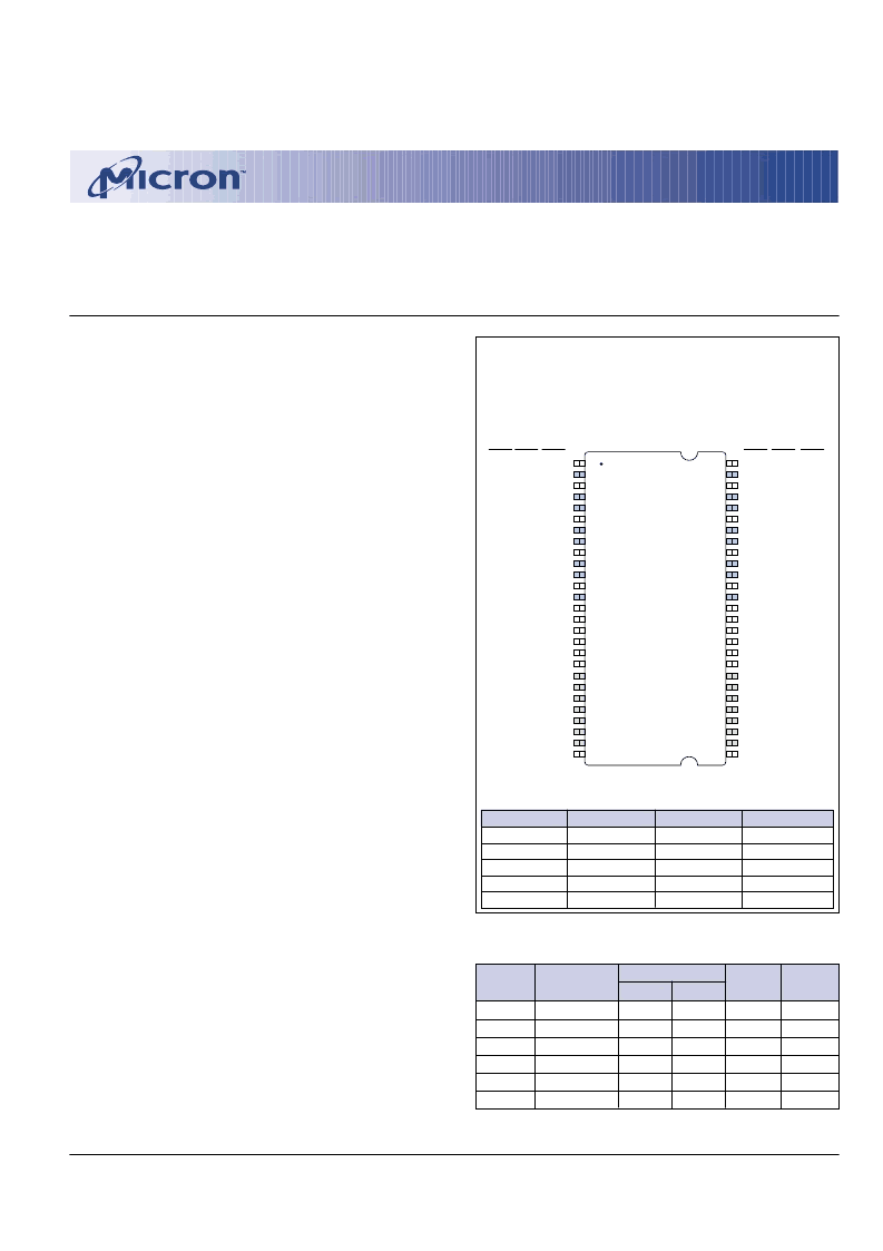
PIN ASSIGNMENT (Top View)
54-Pin TSOP
FEATURES
PC100-, and PC133-compliant
Fully synchronous; all signals registered on positive
edge of system clock
Internal pipelined operation; column address can be
changed every clock cycle
Internal banks for hiding row access/precharge
Programmable burst lengths: 1, 2, 4, 8, or full page
Auto Precharge, includes CONCURRENT AUTO
PRECHARGE, and Auto Refresh Modes
Self Refresh Mode; standard and low power
64ms, 4,096-cycle refresh
LVTTL-compatible inputs and outputs
Single +3.3V ±0.3V power supply
OPTIONS
Configurations
32 Meg x 4
16 Meg x 8
8 Meg x 16 (2 Meg x 16 x 4 banks)
WRITE Recovery (
t
WR)
t
WR = “2 CLK”
1
Package/Pinout
Plastic Package – OCPL
2
54-pin TSOP II (400 mil)
60-ball FBGA (8mm x 16mm)
60-ball FBGA (11mm x 13mm)
Timing (Cycle Time)
10ns @ CL = 2 (PC100)
7.5ns @ CL = 3 (PC133)
7.5ns @ CL = 2 (PC133)
Self Refresh
Standard
Low power
Operating Temperature Range
Commercial (0
o
C to +70
o
C)
Industrial (-40
o
C to +85
o
C)
MARKING
(8 Meg x 4
(4 Meg x 8
x 4 banks)
x 4 banks)
32M4
16M8
8M16
A2
TG
FB
3,6
FC
3,6
-8E
3,4,5
-75
-7E
None
L
None
IT
3
Part Number Example:
MT48LC16M8A2TG-7E
NOTE
: 1. Refer to Micron Technical Note: TN-48-05.
2. Off-center parting line.
3. Consult Micron for availability.
4. Not recommended for new designs.
5. Shown for PC100 compatability.
6. See page 59 for FBGA Device Marking Table.
V
DD
DQ0
V
DD
Q
DQ1
DQ2
VssQ
DQ3
DQ4
V
DD
Q
DQ5
DQ6
VssQ
DQ7
V
DD
DQML
WE#
CAS#
RAS#
CS#
BA0
BA1
A10
A0
A1
A2
A3
V
DD
1
2
3
4
5
6
7
8
9
10
11
12
13
14
15
16
17
18
19
20
21
22
23
24
25
26
27
54
53
52
51
50
49
48
47
46
45
44
43
42
41
40
39
38
37
36
35
34
33
32
31
30
29
28
Vss
DQ15
VssQ
DQ14
DQ13
V
DD
Q
DQ12
DQ11
VssQ
DQ10
DQ9
V
DD
Q
DQ8
Vss
NC
DQMH
CLK
CKE
NC
A11
A9
A8
A7
A6
A5
A4
Vss
x8
-
DQ7
-
NC
DQ6
-
NC
DQ5
-
NC
DQ4
-
NC
-
-
DQM
-
-
-
-
-
-
-
-
-
-
-
x16
x16
x8
-
DQ0
-
NC
DQ1
-
NC
DQ2
-
NC
DQ3
-
NC
-
NC
-
-
-
-
-
-
-
-
-
-
-
-
x4
-
NC
-
NC
DQ3
-
NC
NC
-
NC
DQ2
-
NC
-
-
DQM
-
-
-
-
-
-
-
-
-
-
-
x4
-
NC
-
NC
DQ0
-
NC
NC
-
NC
DQ1
-
NC
-
NC
-
-
-
-
-
-
-
-
-
-
-
-
Note:
The # symbol indicates signal is active LOW. A dash (
–
)
indicates x8 and x4 pin function is same as x16 pin function.
KEY TIMING PARAMETERS
SPEED
GRADE
-7E
-7E
-75
-8E
3,4,5
-75
-8E
3 ,4,5
CLOCK
FREQUENCY CL = 2* CL = 3*
143 MHz
133 MHz
133 MHz
125 MHz
100 MHz
100 MHz
ACCESS TIME
SETUP
TIME
1.5ns
1.5ns
1.5ns
2ns
1.5ns
2ns
HOLD
TIME
0.8ns
0.8ns
0.8ns
1ns
0.8ns
1ns
–
5.4ns
–
5.4ns
6ns
–
–
5.4ns
–
–
6ns
6ns
*CL = CAS (READ) latency
相關(guān)PDF資料 |
PDF描述 |
|---|---|
| MT48LC8M16A2FC-7EIT | SYNCHRONOUS DRAM |
| MT48LC8M16A2FC-7EL | SYNCHRONOUS DRAM |
| MT48LC8M16A2FC-7ELIT | SYNCHRONOUS DRAM |
| MT48LC8M16A2FC-8E | SYNCHRONOUS DRAM |
| MT48LC8M16A2FC-8EIT | SYNCHRONOUS DRAM |
相關(guān)代理商/技術(shù)參數(shù) |
參數(shù)描述 |
|---|---|
| MT48LC8M16A2FC-7EIT | 制造商:MICRON 制造商全稱:Micron Technology 功能描述:SYNCHRONOUS DRAM |
| MT48LC8M16A2FC-7EL | 制造商:MICRON 制造商全稱:Micron Technology 功能描述:SYNCHRONOUS DRAM |
| MT48LC8M16A2FC-7ELIT | 制造商:MICRON 制造商全稱:Micron Technology 功能描述:SYNCHRONOUS DRAM |
| MT48LC8M16A2FC-8E | 制造商:MICRON 制造商全稱:Micron Technology 功能描述:SYNCHRONOUS DRAM |
| MT48LC8M16A2FC-8EIT | 制造商:MICRON 制造商全稱:Micron Technology 功能描述:SYNCHRONOUS DRAM |
發(fā)布緊急采購,3分鐘左右您將得到回復(fù)。