- 您現(xiàn)在的位置:買賣IC網(wǎng) > PDF目錄384755 > MT48LC64M8A2 (Micron Technology, Inc.) SYNCHRONOUS DRAM PDF資料下載
參數(shù)資料
| 型號: | MT48LC64M8A2 |
| 廠商: | Micron Technology, Inc. |
| 英文描述: | SYNCHRONOUS DRAM |
| 中文描述: | 同步DRAM |
| 文件頁數(shù): | 26/55頁 |
| 文件大?。?/td> | 1828K |
| 代理商: | MT48LC64M8A2 |
第1頁第2頁第3頁第4頁第5頁第6頁第7頁第8頁第9頁第10頁第11頁第12頁第13頁第14頁第15頁第16頁第17頁第18頁第19頁第20頁第21頁第22頁第23頁第24頁第25頁當前第26頁第27頁第28頁第29頁第30頁第31頁第32頁第33頁第34頁第35頁第36頁第37頁第38頁第39頁第40頁第41頁第42頁第43頁第44頁第45頁第46頁第47頁第48頁第49頁第50頁第51頁第52頁第53頁第54頁第55頁
26
512Mb: x4, x8, x16 SDRAM
512MSDRAM_D.p65
–
Rev. D; Pub 1/02
Micron Technology, Inc., reserves the right to change products or specifications without notice.
2000, Micron Technology, Inc.
512Mb: x4, x8, x16
SDRAM
ADVANCE
CLK
DQ
T2
T1
T4
T3
T6
T5
T0
COMMAND
WRITE - AP
BANK
n
NOP
NOP
NOP
NOP
D
IN
a
+ 1
D
IN
a
NOP
NOP
T7
BANK
n
BANK
m
ADDRESS
NOTE:
1. DQM is LOW.
BANK
n
,
COL
a
BANK
m
,
COL
d
READ - AP
BANK
m
Internal
States
t
Page Active
WRITE with Burst of 4
Interrupt Burst, Write-Back
Precharge
Page Active
READ with Burst of 4
t
tRP - BANK
m
D
OUT
d
D
OUT
d
+ 1
CAS Latency = 3 (BANK
m
)
RP - BANK
n
WR - BANK
n
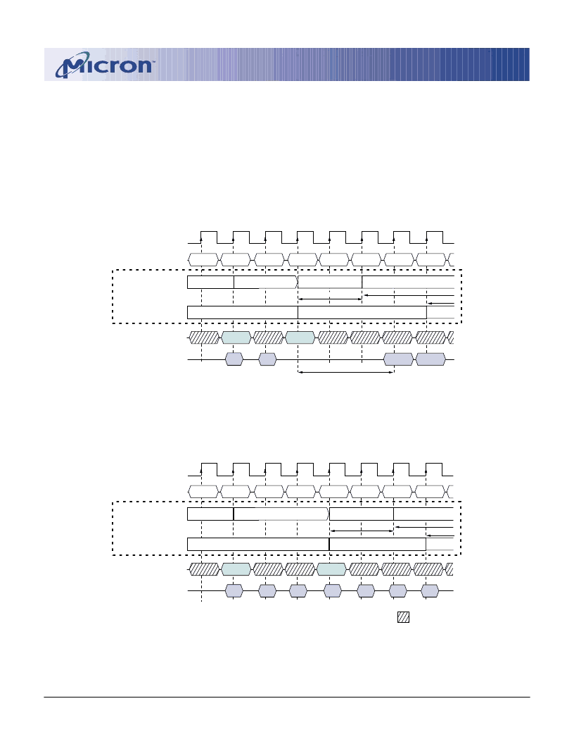
Figure 26
WRITE With Auto Precharge Interrupted by a READ
DON
’
T CARE
CLK
DQ
T2
T1
T4
T3
T6
T5
T0
COMMAND
WRITE - AP
BANK
n
NOP
NOP
NOP
NOP
D
IN
d
+ 1
D
IN
d
D
IN
a
+ 1
D
IN
a
+ 2
D
IN
a
D
IN
d
+ 2
D
IN
d
+ 3
NOP
T7
BANK
n
BANK
m
ADDRESS
NOP
NOTE:
1. DQM is LOW.
BANK
n
,
COL
a
BANK
m
,
COL
d
WRITE - AP
BANK
m
Internal
States
t
Page Active
WRITE with Burst of 4
Interrupt Burst, Write-Back
Precharge
Page Active
WRITE with Burst of 4
Write-Back
WR - BANK
n
tRP - BANK
n
tWR - BANK
m
Figure 27
WRITE With Auto Precharge Interrupted by a WRITE
WRITE with auto precharge
3. Interrupted by a READ (with or without AUTO
PRECHARGE): A READ to bank
m
will interrupt a
WRITE on bank
n
when registered, with the data-out
appearing CAS latency later. The PRECHARGE to bank
n
will begin after
t
WR is
met, where
t
WR begins when
the READ to bank
m
is registered. The last valid WRITE
to bank
n
will be data-in registered one clock prior to
the READ to bank
m
(Figure 26).
4. Interrupted by a WRITE (with or without auto
precharge): A WRITE to bank
m
will interrupt a WRITE
on bank
n
when registered. The PRECHARGE to bank
n
will begin after
t
WR is met, where
t
WR begins when
the WRITE to bank
m
is registered. The last valid data
WRITE to bank
n
will be data registered one clock
prior to a WRITE to bank
m
(Figure 27).
相關(guān)PDF資料 |
PDF描述 |
|---|---|
| MT48LC32M16A2 | SYNCHRONOUS DRAM |
| MT48LC8M16A2FB-75LIT | SYNCHRONOUS DRAM |
| MT48LC8M16A2FB-7E | SYNCHRONOUS DRAM |
| MT48LC8M16A2FB-7EIT | SYNCHRONOUS DRAM |
| MT48LC8M16A2FB-7EL | SYNCHRONOUS DRAM |
相關(guān)代理商/技術(shù)參數(shù) |
參數(shù)描述 |
|---|
發(fā)布緊急采購,3分鐘左右您將得到回復。